
Professional PCB manufacturing and assembly
Building 6, Zone 3, Yuekang Road,Bao'an District, Shenzhen, China
+86-13410863085Mon.-Sat.08:00-20:00

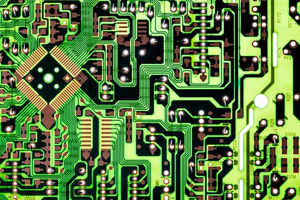
High Density PCB Circuit Board Technology and Application
High-density circuit board technology is a key technology in the field of modern circuit board design and manufacturing. It enables more circuit components to be integrated on the circuit board by increasing the number of board layers, reducing the spacing of components, and adopting high-precision technology. for higher performance and smaller size. This article will discuss the principle, design and production process, quality control and other aspects of high-density circuit board technology, as well as its application in electronics, communications, aerospace and other industries.
1. The principle and development process of high-density circuit board technology
High-density circuit board technology refers to densely laying out more circuit components, signal lines and power lines on the circuit board through certain technical means to achieve higher performance and smaller size. With the rapid development of digitization, informatization and intelligence, the requirements for the size, weight, power consumption and performance of electronic products are getting higher and higher, which puts forward higher requirements for circuit board technology. High-density circuit board technology has emerged as the times require, which can greatly reduce the size of the circuit board, improve the signal transmission rate, anti-interference ability and service life of the circuit board, and at the same time improve production efficiency and reduce costs.
The development of high-density circuit board technology can be traced back to the 1960s. At that time, IBM Corporation of the United States first developed the world's first high-density printed circuit board, which used four layers of copper foil, and the line width and line distance were only 0.025mm, which realized a qualitative leap in industrial production at that time. Subsequently, Japan's NEC Corporation also began to develop high-density circuit boards, and began to apply them in electronic products such as mobile phones and notebook computers in the late 1970s. Since the 21st century, high-density circuit board technology has developed rapidly in more advanced and efficient forms, such as ultra-thin cross-layer boards, inner layer perforation, micro-hole/blind-hole technology, etc., which have greatly improved the three-dimensional density and performance level.
2. Design and production process of high-density circuit board
The design and production process of high-density circuit boards is relatively complicated, and requires careful planning, design, manufacturing and quality control of multiple links. Among them, the design of high-density circuit boards is the basis for efficient manufacturing, and it is also the core of correcting problems and errors. Its specific process includes:
1. Layout design: Arrange the layout of components in the circuit according to the actual size of the circuit, the distribution of chip pins and other factors.
2. Circuit design: It is the core for the designer to determine the line width, line spacing, plate thickness specification, plate selection and plate number and other factors.
3. Verify the design: After the design is completed, it is necessary to conduct circuit simulation and verification through professional circuit board CAD software. Faced with the most salient issues, the most appropriate resolution is reached and both parties will reach an agreed settlement.
4. Manufacture and production: After the verification process, the circuit board design documents are transferred to the circuit board manufacturing factory, and then manufactured through a series of processing processes, finally forming a finished high-density circuit board.
5. Testing and inspection: After the manufacturing is completed, a series of tests such as electrical performance testing, welding quality testing, metal coating thickness testing, and surface quality testing need to be performed on the circuit board to ensure that the high-density circuit board can meet the designed performance requirements.
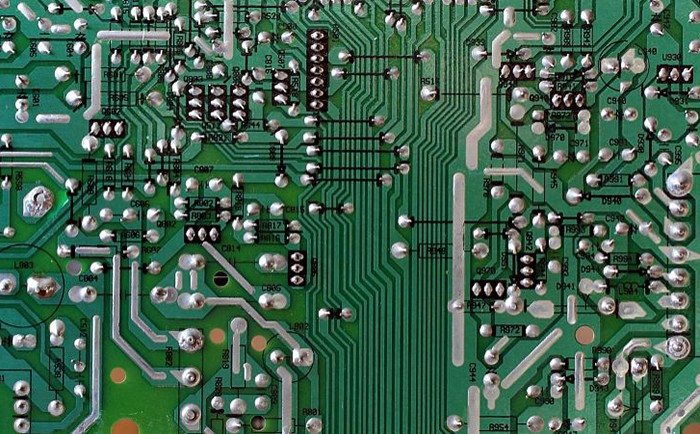
3. Methods and technologies for quality control of high-density circuit boards
In the manufacturing process of high-density circuit boards, quality control is also a very important part. At present, the main quality control technologies used in the industry are:
1. AOI (Automatic Optical Inspection) automatic optical inspection: AOI technology uses an optical camera to take high-precision image photos, and then conducts automatic inspections to detect whether the position of circuit board components is accurate, whether the welding quality is good, whether the linear accuracy and other factors are correct. Up to standard.
2. E-test (Electric Test) electrical test: E-test technology is to conduct electrical tests on the circuit board to determine whether the circuit is on and off, the interconnection mode and mutual polarity, etc., that is, to check the high-density circuit board to achieve Whether the conduction performance meets the requirements.
3. X-ray inspection: X-ray inspection is mainly used to check whether the position and layout of the internal components of the circuit board meet the requirements, as well as the position of the inner hole and whether it is penetrated, etc., to prevent the occurrence of concealment problems and improve the quality of the circuit board. reliability.
4. Application of high-density circuit boards in electronics, communications, aerospace and other industries
High-density circuit board technology is widely used, and has been widely used in electronics, communications, aerospace and other industries. For example, high-density circuit boards can be used to manufacture light-concentrating and circuit-integrated equipment, or as core components such as switches, routers, and data center servers in computers and communication engineering, and can also be used to manufacture drones, water In aerospace equipment such as robots.
5. Future trends and prospects of high-density circuit board technology
It is expected that high-density circuit board technology will further develop in the future, mainly focusing on the following directions:
1. Improvement of transmission rate: Using more advanced technology and material technology, the clock frequency of high-density circuit boards is expected to be raised to a higher level to meet the demand for increased data transmission.
2. Energy saving and consumption reduction: As energy consumption becomes a focus of countries all over the world, high-density circuit board technology is expected to be more applied to corresponding equipment to achieve high-efficiency and low-consumption operation in the industry.
3. Wireless interconnection: The continuous popularization of concepts such as smart home and smart city will greatly promote the iteration of high-density circuit board technology. This technology will continue to develop in the direction of wireless interconnection and bring people a more convenient life.
High-density circuit board technology is a technology that has attracted much attention in the field of electronics manufacturing. By reducing size, improving performance, and enhancing reliability, etc., it meets the requirements of modern electronic equipment with smaller size, higher economy, and stronger performance requirements. growing demand. With the continuous development of technology, the application field of high-density circuit board technology is becoming wider and wider, which also means that its future development trend is more extensive
PCB demand analysis of new energy vehicles
May 30,2023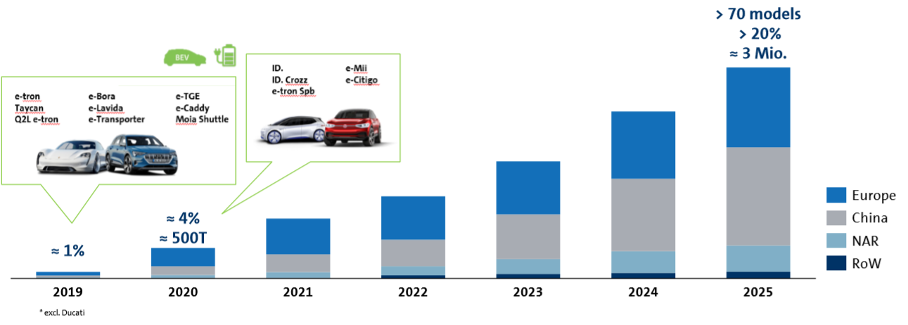


Just upload Gerber files, BOM files and design files, and the KINGFORD team will provide a complete quotation within 24h.