
Professional PCB manufacturing and assembly
Building 6, Zone 3, Yuekang Road,Bao'an District, Shenzhen, China
+86-13410863085Mon.-Sat.08:00-20:00

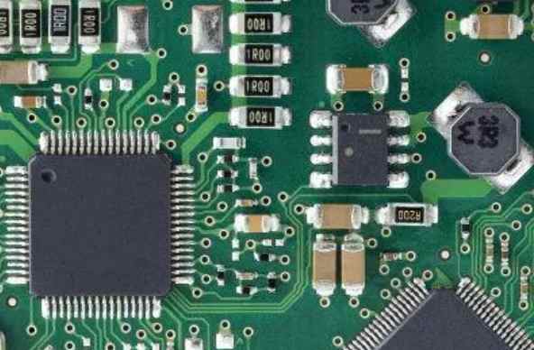
PCB electronic components can be divided into discrete components and integrated components. Integrated components should be preferred in the design of electronic systems, because integrated components have good sealing, fewer solder joints and strong anti-interference line, and the device with slow signal slope can reduce the influence of high frequency components on the circuit. The use of patch components can shorten the distance of connecting wires, reduce the impedance value, which is conducive to improving electromagnetic compatibility.
PCB board components selection and layout
Component layout, the incompatible components are separated to ensure the interference between components, and attention should be paid to the following problems: component layout to meet the mechanical structure of the system positioning, the device to be strictly located such as sensors, transformers, monitors and other fixed positions, heating components should be installed and away from the integrated circuit, placed at the edge of the PCB circuit board, In the case of high frequency, PCB board lead, through hole, distributed capacitance has a great impact on the circuit, so the design should minimize the line distance, the interference generated by the power supply is more serious, the decoupling capacitor of integrated circuit chip is better to adopt the form of patch, so that the lead is shorter, less interference.
Circuit board type and components selection, layout, all to consider is the wiring of the circuit board, the principle is to try to connect the line as short as possible. In order to reduce the introduction of additional interference signals, generally first cloth clock line, sensitive component signal line, then cloth high-speed signal line, and finally cloth generally not important signal line.

Consider the above principles, but also pay attention to the problem: when the multi-layer circuit board wiring, the two adjacent layers between the well layout structure, reduce the bending of the line, in order to prevent changes in impedance value, signal line bend designed into a circular arc.
The outermost wire or device of the PCB circuit board should be no less than 2mm away from the edge of the circuit board, which is conducive to the fixing of the PCB board and prevent the change of impedance value. The wire is small and short, which is conducive to anti-interference. Considering the resistance of the wire and the current flowing through, the width of the wire is generally between 1 and 1.5mm to meet the requirements.
Circuit boards and classifications, features and application areas are introduced
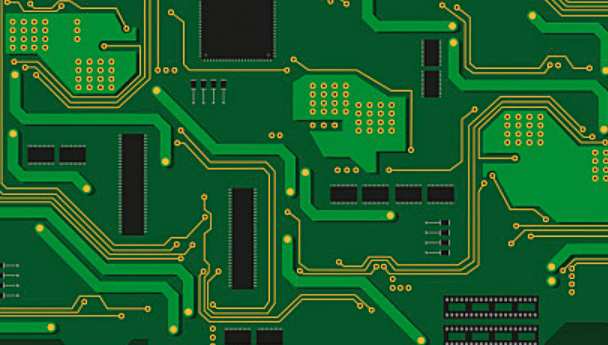
Circuit board names are: circuit board, PCB circuit board, aluminum substrate, high frequency board, thick copper board, impedance board, PCB, ultra-thin circuit board, ultra-thin circuit board, printing (copper etching technology) circuit board, etc. The circuit board makes the circuit miniaturized and intuitive, which plays an important role in the mass production of fixed circuit and the optimization of electrical appliance layout. A Circuit Board can be called a Printed Circuit Board or a printed circuit board, the English name is printed Circuit Board (PCB).
Circuit boards according to the number of layers to be divided into single panel, double panel, and multilayer circuit boards three big classification.
The first is the single panel. On the most basic PCB, the parts are concentrated on one side and the wires on the other. This type of PCB is called a single-sided circuit board because the wires appear on only one side. Single panels are usually simple and inexpensive to make, but the disadvantage is that they cannot be used on complex products.
Dual panel is an extension of single panel, when single-layer wiring can not meet the needs of electronic products, dual panel will be used. Both sides are covered with copper and have a route, and the line between the two layers can be guided through the hole, so that it forms the required network connection.
The multilayer board refers to a printed board with more than three layers of conductive graphics layers and insulating materials in between, and the conductive graphics in between are interconnected as required.
Multilayer circuit board is electronic information technology to high speed, multi-function, large capacity, small volume, thin, clear direction of the product development.
Circuit board according to the characteristics of the words are divided into soft board (FPC), high precision single and double circuit board, soft and hard combined board (FPCB).
Precautions for installing molds when blanking single-side circuit board
1. Select the punching press (including type and tonnage) according to the punching force, mold size and closing height calculated by mold design.
2. Start the punch, a comprehensive check including clutch, brake, slider and other parts are normal, whether the operating mechanism can be perfect, never even impact phenomenon.
3. The cushion iron under the punching die, usually 2 pieces, must be ground out at the same time on the grinder, to ensure that the mold installation is parallel and vertical. The interposition of the cushion is not to obstruct the blanking while being as close to the center of the mold as possible.
4. Several sets of pressure plates and T-head pressure plate screws should be prepared for corresponding use with the mold. The front end of the platen should not touch the straight wall of the lower die. Emery cloth should be placed between each contact surface, and screws must be tightened. Metal base core board
5. During mold installation, we should pay great attention to the screws and nuts on the lower die not touching the upper die (the upper die falls and closes).
6. Adjust the mold as much as possible with manual, not manual.
7. In order to improve the blanking performance of the substrate, the paper substrate should be heated. Its temperature to 70 ~ 90℃ is better.
What is the FPC circuit board
FPC is short for Flexible Printed Circuit, also known as soft printed circuit board, flexible printed circuit board, flexible circuit board, referred to as soft board or FPC, has the characteristics of high wiring density, light weight, thin thickness.
It is mainly used in many products such as mobile phones, laptops, PDAs, digital cameras, and LCM.
FPC flexible printed circuit is a high frequency plate or polyester film as the substrate made of a high reliability, excellent flexibility printed circuit.
Product features:
1. It can be bent, folded and wound freely, and can be moved and expanded freely in three-dimensional space.
2. Good heat dissipation performance, F-PC can be used to reduce the volume.
3. Realize lightweight, miniaturization and thin shape, so as to achieve the integration of component device and wire connection.


Just upload Gerber files, BOM files and design files, and the KINGFORD team will provide a complete quotation within 24h.