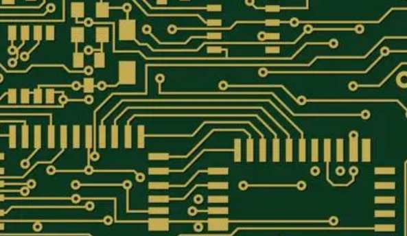
Many designers believe that reducing line length is the key to reducing crosstalk. In fact, almost all circuit design software provides the maximum parallel line length control function. Unfortunately, it's very difficult to reduce crosstalk just by changing the geometry.
Because forward crosstalk is affected by coupling length, there is little reduction in crosstalk when you shorten the length of a line that has no coupling relationship. Moreover, if the coupling length exceeds the driver chip down or up delay, the linear relationship between the coupling length and the forward crosstalk will reach a saturation value, at which point, shortening the already long coupling line has little effect on crosstalk reduction.
A reasonable approach is to widen the distance between the coupling lines. In almost all cases, decoupling coupling lines can greatly reduce crosstalk interference. It turns out that the backward-crosstalk amplitude is roughly inversely proportional to the square of the distance between the coupling lines, i.e., if you double the distance, the crosstalk decreases by three-quarters. This effect is more pronounced when backward crosstalk is predominant.
Isolation difficulty
It is not easy to increase the distance between the coupled lines. If you have very dense wiring, you have to put a lot of effort into reducing it. If you're worried about crosstalk interference, you can add one or two layers of isolation. If you have to increase the distance between lines or networks, you'd better have software that's easy to use. The width and thickness of the line also affect crosstalk interference, but the effect is much less than the distance factor of the line. As a result, these two parameters are rarely adjusted.
Since the dielectric constant of the circuit board insulation material will also generate coupling capacitance between the lines, reducing the dielectric constant can also reduce crosstalk interference. This effect is not obvious, especially since part of the microstrip circuit's dielectric is already air. What's more, changing the dielectric constant is not that easy, especially in expensive equipment. A workaround would be to use a more expensive material instead of FR-4.
Dielectric thickness and length greatly affect crosstalk interference. In general, placing the wiring layer close to the power layer (Vcc or ground) can reduce crosstalk interference. The exact value of the improvement needs to be determined by simulation.
Stratification factor
Some PCB designers still do not pay attention to layering, which is a major failure in high-speed circuit design. Layering not only affects the performance of the transmission line, such as impedance, delay and coupling, but also the circuit is prone to aberration or even change. For example, crosstalk interference can be reduced by reducing dielectric thickness by 5mil, which is not possible, although it can be done in cost and process.

Another factor that is easy to overlook is the choice of layers. In many cases, forward crosstalk is the main crosstalk interference in microstrip circuits. However, if the design is correct, the wiring layer is located between the two power layers, so that there is a good balance between capacitive and inductive coupling, and backward crosstalk with low amplitude becomes the main factor. So, when you simulate, you have to pay attention to what kind of crosstalk interference is dominant.
Wiring and chip placement also have an effect on crosstalk. The location and performance of the driver chip are very important because the backward crosstalk reaches the receiver chip and reflects back to the driver chip. Because of the complexity of the topology, reflection, and other factors, it is difficult to explain who is primarily responsible for crosstalk. If there are multiple topologies to choose from, it is best to use simulation to determine which structure has the least impact on crosstalk.
One non-geometric factor that may reduce crosstalk is the technical specifications of the driver chip itself. As a general rule, choose drivers with long switching times to reduce crosstalk interference (as well as many other problems caused by high speeds). Even if crosstalk is not strictly proportional to switching time, reducing switching time can still have a significant impact. Many times, you have no choice about the driver technology, you have to change the geometric parameters to achieve this.
Reduce crosstalk through the terminal
It is well known that a terminal connection of an independent, uncoupled transmission line matches the impedance and it produces no reflection. Now consider a series of coupled transmission lines, for example, three transmission lines that have crosstalk with each other, or a pair of coupled transmission lines. If circuit analysis software is used, a pair of matrices can be derived representing the capacitance and inductance of the transmission lines themselves and between them. For example, three transmission lines might have the following C and L matrices:
In these matrices, the diagonal elements are the values of the transmission lines themselves, and the non-diagonal elements are the values of the transmission lines to each other. (Note that they are expressed in pF and nH per unit length). These values can be determined by a good electromagnetic field tester.
It can be seen that each set of transmission lines also has a characteristic impedance matrix. In this Z0 matrix, the diagonal elements represent the impedance values of the transmission line to the ground, and the non-diagonal elements are the transmission line coupling values.
For a set of transmission lines, similar to a single transmission line, the matrix is almost identical if the terminal is an impedance matrix matching Z0. The required impedance does not have to be the value in Z0, as long as the composed impedance network matches Z0. The impedance matrix includes not only the impedance of the transmission line to the ground, but also the impedance between the transmission lines.
Such an impedance matrix has good properties. First, it prevents crosstalk reflection in uncoupled lines. More importantly, it can eliminate the crosstalk that has been formed.
Deadly weapon
Unfortunately, such a terminal is expensive and impossible to implement ideally, because the coupling impedance between some transmission lines is too small, resulting in large currents flowing into the driver chip. The impedance between the transmission line and the ground should not be so great that it cannot drive the chip. If these problems exist, and you intend to use such terminals, add a few AC coupling capacitors.
Despite some implementation difficulties, impedance array terminals are a lethal weapon against signal reflection and crosstalk, especially in harsh situations. It may or may not work in other Settings, but it is still a recommended approach.


