
Professional PCB manufacturing and assembly
Building 6, Zone 3, Yuekang Road,Bao'an District, Shenzhen, China
+86-13410863085Mon.-Sat.08:00-20:00


In the rapid development of today, automotive electronics, industrial manufacturing, medical equipment and technology enterprises have tended to intelligent development, intelligent products for engineering research and development ability to improve the test, the manufacturing process also has very strict requirements and standards, and as an important electronic circuit board in electronic products, is an important part of product operation. The quality of the circuit board will also affect the working efficiency of the product, and even affect the life safety. So, when we design the circuit board of a product, what knowledge should we know? Jingbang Electronics, a 12-year professional SMT processing factory, is here to tell you about the relationship between SMD, SMT and BOM in the processing of the circuit board.
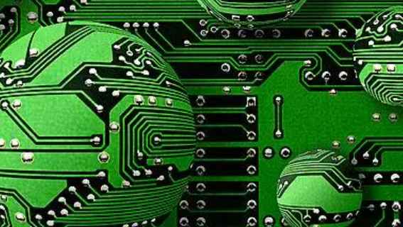
SMT is Surface assembly Technology, also known as Surface Mounted Technology, (abbreviation of Surface Mounted technology), is the most popular technology and process in the electronic assembly industry.
SMT: surface mounted technology (surface Mounted technology): The ability to directly attach the components to the surface and weld them to the regular position of the PCB surface.
SMD: Abbreviation of Surface Mounted Devices, meaning: Surface Mounted Devices, it is one of the SMT components. There are many kinds, such as chip resistance, chip capacitance, chip triode, chip inductance and so on.
The shape of the SMD is rectangular sheet, cylindrical row or shaped, and the welding end or pin is manufactured in the same plane, and it is suitable for Reflow of the electronic components attached by the external patch machine soldering(reflow soldering): Weld the solder paste pre-distributed on the PCB board welding pad from the top to complete the mechanical and electrical connection between the component terminals or pins attached externally and the printed circuit board welding pad.

Chip: rectangular chip component: rectangular surface adhesive component with no lead at both ends and welded end.
SOP: small outline package(IC): An exterior assembly component in a small moulded plastic package with short wing or J-shaped pins on either side.
QFP: quad flat pack (quad flat pack IC) : quadrilateral with airfoil short pin, pin distance: 1.00, 0.80, 0.65, 0.50, 0.40, 0.30 mm placement machine plastic packaging such as integrated circuit IC.
BGA: Ball grid array: Package of integrated circuits in which the input and output points are tin balls arranged in a grid pattern on the underside of the component.
SMT and SMD apply the waste water produced after commodity cleaning in the production process in the surface mounting skills, bringing pollution of water quality, earth and animals and plants. In addition to water cleaning, the use of chlorofluorocarbon-rich organic solvents (CFCS & HCFCS) for cleaning also causes pollution and damage to the air and atmosphere. Cleaning agent residue on the machine board brings corrosion appearance, seriously affect the quality of goods. Reduce cleaning operation and machine protection costs. No cleaning can reduce the damage caused by PCBA during movement and cleaning. There are still some components that cannot be cleaned.
The flux residue has been controlled and can be used to cooperate with the appearance requirements of goods to prevent visual inspection of the cleaning condition. The residual flux has been continuously improved in its electrical function to prevent leakage of electricity from the product, resulting in any damage. The wash-free process has passed a number of international safety tests, proving that the chemical substances in the solder flux of smt SMT machine are stable and non-corrosive.
BOM: Bill of Material (BOM), the use of computer-aided enterprise production management, first of all, to enable the computer to read the composition of the products produced by the enterprise and all the materials involved, in order to facilitate computer identification, must be the product structure expressed in graphic format into a certain data format. The document that describes the product structure in data format is the bill of Materials, or BOM, which is the technical document that defines the product structure.
Therefore, it is also called product structure table or product structure tree. In some industries, this may be called a "recipe," "factor list," or some other name. In MRPⅡ and ERP system, the word material has a wide meaning, it is all products, semi-finished products, products in process, raw materials, accessories, collaborative parts, consumables and other product-related materials collectively.


Just upload Gerber files, BOM files and design files, and the KINGFORD team will provide a complete quotation within 24h.