
Professional PCB manufacturing and assembly
Building 6, Zone 3, Yuekang Road,Bao'an District, Shenzhen, China
+86-13410863085Mon.-Sat.08:00-20:00


If EMI is to be minimized, keep the signal line as close as possible to the return signal line formed with it, so that the loop area is as small as possible to avoid radiation interference. The low level signal channel should not be near the high level signal channel and the unfiltered power line. The wiring sensitive to noise should not be parallel to the high current and high speed switching line. If possible, lay out all the key routes in strips. Incompatible signal lines (digital and analog, high speed and low speed, high current and low current, high voltage and low voltage, etc.) should be kept away from each other and not run parallel. The crosstalk between signals is very sensitive to the length and distance of adjacent parallel cables. Therefore, the distance between high-speed signal cables and other parallel signal cables should be widened and the parallel length should be narrowed.
The inductance of a guide band is proportional to the logarithm of its length and length and inversely proportional to the logarithm of its width. Therefore, the guide tape should be as short as possible, each address line or data line of the same component should maintain the same length as far as possible, as the input and output wires of the circuit should avoid parallel adjacent, it is best to add a ground line between them, which can effectively inhibit crosstalk. Low speed signal wiring density can be relatively large, high speed signal wiring density should be as small as possible.
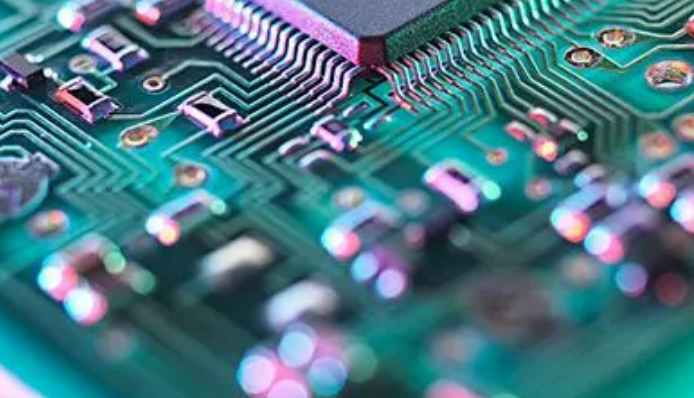
In the multilayer thick film process, besides obeying the rules of single-layer wiring, attention should also be paid to:

Try to design a separate ground surface, signal layer arrangement and the ground adjacent. When not in use, a ground wire must be placed near the high frequency or sensitive circuit. The strike of signal lines distributed in different layers should be perpendicular to each other, which can reduce the electric field and magnetic field coupling interference between lines. The signal line on the same layer to maintain a certain distance, it is best to use the corresponding ground circuit isolation, reduce signal crosstalk between lines. Every high-speed signal line should be restricted to the same level. The signal line should not be too close to the edge of the substrate, otherwise it will cause characteristic impedance changes, and it is easy to produce edge field, increasing the outward radiation.
4, the layout of the clock line
Clock circuit plays an important role in digital circuit and is the main source of electromagnetic radiation. A clock signal with a 2ns rising edge radiates energy up to 160MHz. Therefore, the design of clock circuit is the key to ensure the electromagnetic compatibility of the whole circuit. Regarding the layout of the clock circuit, there are the following considerations:
(1) Do not use the Daisy chain structure to transmit the clock signal, but should use the star structure, that is, all the clock load directly connected to the clock power driver.
(2) The guide band connecting the input/output terminal of crystal oscillator should be as short as possible to reduce noise interference and the influence of distributed capacitance on crystal oscillator.
(3) crystal oscillator capacitor ground wire should be connected to the device with as wide and short a guide band as possible; The digital ground pin closest to the crystal oscillator should minimize overhole.
Three, the selection of technology and components
There are three manufacturing processes available for hybrid integrated circuits: single-layer film, multilayer thick film and multilayer co-fired thick film. The thin-film process is capable of producing components of small size, low power and high current density required for high-density hybrid circuits. It has the characteristics of high quality, stability, reliability and flexibility, and is suitable for high-speed high-frequency and high package density circuits. But can only do single layer wiring and high cost. Multilayer thick film technology can produce multilayer interconnect circuits at a lower cost. From the perspective of electromagnetic compatibility, multilayer wiring can reduce the electromagnetic radiation of circuit boards and improve the anti-interference ability of circuit boards. Because special power layers and strata can be set up, the distance between the signal and the ground wire is only the interlayer distance. In this way, the loop area of all signals on the board can be reduced to a minimum, thus effectively reducing the differential mode radiation.
The multilayer co-fired thick film technology has more advantages and is the mainstream technology of passive integration at present. It can realize more layers of wiring, easy to embed components, improve assembly density, has good high-frequency characteristics and high-speed transmission characteristics. In addition, the hybrid multilayer circuit with higher assembly density and better performance can be achieved by the combination of the two.
Active devices in hybrid circuits generally use bare chips. If there is no bare chip, the corresponding packaged chip can be used. In order to obtain the best EMC characteristics, the surface chip should be used as far as possible. Choose the low speed clock as far as possible under the premise of meeting the technical specifications of the product. Never use AC when HC is available, and never use HC when CMOS4000 is available. The capacitor should have a low equivalent series resistance so as to avoid large attenuation of the signal.
The package of hybrid circuit can adopt the base and cover of cutting metal, parallel seam welding, with good shielding effect.


Just upload Gerber files, BOM files and design files, and the KINGFORD team will provide a complete quotation within 24h.