
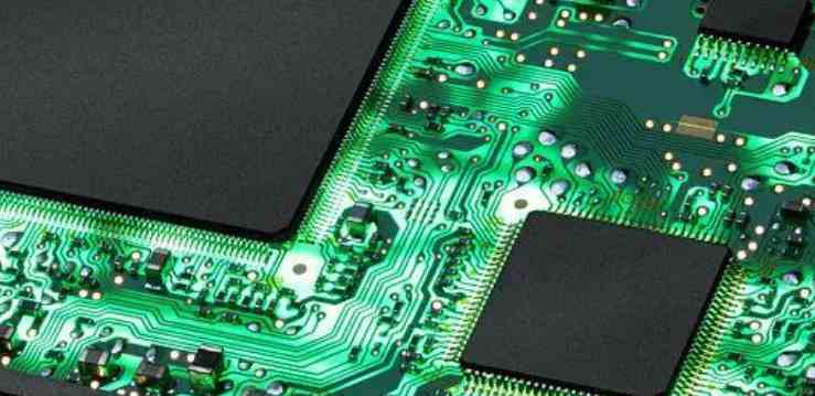
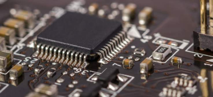
Professional PCB manufacturing and assembly
Building 6, Zone 3, Yuekang Road,Bao'an District, Shenzhen, China
+86-13410863085Mon.-Sat.08:00-20:00

1. The baking temperature shall not exceed the Tg point of PCB, and the general requirement shall not exceed 125℃. In the early days, the Tg point of some PCBS containing lead was relatively low. Now, the Tg of most PCBS without lead is above 150℃.
2, the baked PCB should be used as soon as possible, if not used, should be re-vacuum packaging as soon as possible. If exposed to the workshop for too long, it must be baked again.
3. Remember to install air pumping and drying equipment in the oven, otherwise the steam baked out will be retained in the oven to increase its relative humidity, which is not conducive to PCB dehumidification.
4. From the point of view of quality, the more fresh PCB solder is used after the furnace, the better the quality is. Even if the expired PCB is used after baking, there will still be a certain quality risk.
Suggestions for PCB baking

1, it is recommended to use as long as 105±5℃ temperature to bake PCB, because the boiling point of water is 100℃, as long as it exceeds the boiling point, water will become water vapor. Since PCBS don't contain too many water molecules, they don't need too much heat to increase the speed of vaporization.
If the temperature is too high or the gasification speed is too fast, it is easy to make the water vapor expand quickly, which is not good for the quality, especially for the multilayer board and PCB with buried holes. 105℃ is just above the boiling point of water, and the temperature is not too high, which can dehumidification and reduce the risk of oxidation. And today's ovens have much better temperature control than before.
2. Whether PCB needs to be baked should be seen whether its packaging is damp, that is, to observe whether the Humidity Indicator Card (HIC) in the vacuum packaging has been shown to be damp. If the packaging is good, the humidity indicator card has not been shown to be damp, it can be directly put on the line without baking.
3, PCB baking is recommended to use the "upright" and interval to bake, because this can play the maximum effect of hot air convection, and water is easier to bake out from the PCB. But for large size PCB may have to consider whether the upright type will cause bending deformation problem.
4, PCB baking is recommended to be placed in a dry place and make it fast cooling, it is best to press on the top of the board "anti-bending fixture", because the general object from the high heat state to the process of cooling but easy to absorb water, but rapid cooling and may cause the plate bending, which should achieve a balance.
PCB baking shortcomings and matters to consider
1. Baking will accelerate the oxidation of PCB surface coating, and the higher the temperature of baking for longer, the more unfavorable.
2, it is not recommended to do high temperature baking on the OSP surface treatment board, because the OSP film will degrade or fail due to high temperature. If you have to do baking, it is recommended to use 105±5℃ temperature baking, not more than 2 hours, after baking it is recommended to use up within 24 hours.
3, baking may have an impact on the generation of IMC, especially for HASL(spray tin), ImSn(chemical tin, dipping tin) surface treatment of the board, because its IMC layer (copper tin compound) has been generated early in the PCB stage, that is, before PCB solder has been generated, baking will increase the thickness of this layer has been generated IMC, Creates trust issues.
Multi - substrate is a high - performance, high - speed system. At higher frequencies, the rise time of the signal is reduced, so the control of signal reflection and line length becomes critical. In multi-substrate system, the controllable impedance performance of electronic components is very strict, and the design should meet the above requirements. The factors that determine the impedance are the dielectric constant of the substrate and the prepreg material, the wire spacing on the same plane, the thickness of the interlayer medium and the thickness of the copper conductor. In high-speed applications, the order of the lamination of the conductors in the multi-substrate and the order of the connection of the signal network are also critical. Dielectric constant: The dielectric constant of the substrate material is an important factor in determining impedance, propagation delay and capacitance.c
The dielectric constant of epoxy resin is 3.45 and that of glass is 6.2. By controlling the percentage of these materials, the dielectric constant of epoxy glass may reach 4.2-5.3. The thickness of the substrate is a good indication for determining and controlling the dielectric constant.
Prepreg materials with relatively low dielectric constant are suitable for application in RF and microwave circuits. In RF and microwave frequencies, lower permittivity causes lower signal delay. In the substrate, the low loss factor minimizes the electrical loss.
The prepreg ROR 4403 is a new material produced by ROGERS. This material is compatible with other substrates used in standard multisubstrate (FR-4 material) structures (for example, RO 4003 or RO 4350 used for microwave boards).


Just upload Gerber files, BOM files and design files, and the KINGFORD team will provide a complete quotation within 24h.