
Professional PCB manufacturing and assembly
Building 6, Zone 3, Yuekang Road,Bao'an District, Shenzhen, China
+86-13410863085Mon.-Sat.08:00-20:00

1. PCB materialused by MITAC at present
A. Urea board
Characteristics: the color is light yellow, often used for single panel, but because it is made of urea paper, easy to rot in cool and humid places, so it is not commonly used now
B. CAM-3 plate
Characteristics: color is milky white, good toughness, high CTI(600V), carbon dioxide emission is only a quarter of the normal. Now it is more commonly used for single panel.
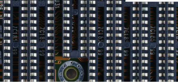
C. FR4 Fiber board
Characteristics: made of fiber, toughness is good, when breaking the wire pull each other, often used in multiple panels, its thermal expansion coefficient is 13(16ppm/c),
D. Multilayer board
Characteristics: high Tg, high heat resistance and low thermal expansion rate, low dielectric constant and dielectric loss materials, mostly used for four layers or more
E. Soft plate
Characteristics: The material is soft, transparent, often used in the electrical connection of two boards, easy to fold, such as laptop LCD and computer main body connection part.
F. Others
With the popularity of multimedia digital information terminal products such as personal computers and mobile phones, PCB is also becoming lighter, thinner, shorter and smaller. Some large foreign companies have developed more PCB boards, such as halogen-free, antimonized environmental protection products, high heat resistance, high Tg boards, low thermal expansion coefficient, low dielectric constant and low dielectric loss boards. The representative products are: FR-5, Tg200 board, PEE board, PI board,CEL-475 and so on. It's just not popular in the country right now
2. The current MITAC PCB-Layout process
A·R&D provides SCHMATIC (EE),FAB OUTLINE (ME) provides schematics and mechanical engineers provide peripheral data
B. Build new parts
We pull out parts from the LIBRARIAN according to the schematic diagram. If there are no such zero parts in the LIBRARIAN, we need to build a new part
C. Parts layout
After the parts are ready, we need to carry out the layout of the parts
D·ROUTING
That's our main job. We set up the board and then we routed it
E. Final finishing
After ROUTING, we will use FABLINK to finally sort out the various materials we need
F· Convert GERBER
GERBER documentation for PC board manufacturers
G· Data storage

After all the work is done, the data is stored for later revision and verification
Iii. Some basic terms about printing plates
On an insulating substrate, conductive graphics of printed lines, printed components, or a combination thereof are made according to a predetermined design, called printed circuits. On an insulating substrate, conductive graphics of electrical connections between components are provided. Printed circuit · It does not include printed components · Printed circuit or printed circuit the finished board is called a printed circuit board or printed circuit board, also called a printed board. Printing board according to the substrate used is rigid or flexible can be divided into two categories: rigid printing brush and flexible printing board. This year has also seen the introduction of rigid - flexible printing plates. According to the number of layers of the conductor pattern can be divided into single-sided, double-sided and multi-layer printing plate. A printed board in which the entire outer surface of a conductor figure is in the same plane as the substrate surface is called a flat plate.
Electronic equipment using printing board, because of the consistency of similar printing board, so as to avoid the error of manual wiring, and can realize the automatic insertion or installation of electronic components, automatic soldering, automatic detection, to ensure the quality of electronic equipment, improve labor productivity, reduce costs, and easy maintenance. Printing boards evolved from single-layer to double-sided, multilayer and flexible, and still have their own trends. Due to the continuous development to the direction of high precision, high density and high reliability, constantly reducing the size, reduce the cost, so that the printing board in the development process of future electronic equipment, still maintain strong vitality.
Those with a total duration of less than 250 seconds are called V-1 FR-4 and those with a total duration of less than 50 seconds are called V-0 FR-4.
Iv. Design process of schematic diagram
The generation of the schematic diagram is generally regarded as the first step of the PCB production process. It is also the concrete realization of the product idea of electronic engineers and technicians. It is composed of many logical components (such as the gate circuit, resistance, capacitance, etc.) through different logical connections. To make a schematic, the source of its logic components is that some CAD software contains a large library of logic components (such as TANGO PADS, etc.). In addition to logic component libraries, some CAD software can also be used by users to create new logic components (such as Cadence,Mentor,Zuken, etc.), so that users can use these logic components to realize the logical functions of the products to be designed.
1) Definition of logical component model (or component name).
2) Encapsulation form of logic component pins
3) Description of pins of logic components
4) Definition of appearance and symbol size of logic components
2 Functions and features of the logical component
To simulate the logic circuit, it is necessary to describe the functional characteristics of each logic component, such as the sequential relationship of the logic component, the initial state RISE, FALL, delay time, drive decay, decay time, etc.
3 Description of the logical component library
Since there are many logic components, it is easy to cause confusion and difficult to manage when they are built under one library. Therefore, logical components with similar functions and characteristics are generally placed under one library and managed according to functional characteristics, such as A/D,D/A conversion devices,CMOS devices, and memory parts. TTL devices, linear devices, operational amplifier devices, comparison devices, etc., are placed separately in the same class library. It can also be categorized by company manufacturer such as MOTOROLA,NEC,INTEL, etc.
Wiring arrangement between PCB components
Mar 14,2023


Just upload Gerber files, BOM files and design files, and the KINGFORD team will provide a complete quotation within 24h.