
Professional PCB manufacturing and assembly
Building 6, Zone 3, Yuekang Road,Bao'an District, Shenzhen, China
+86-13410863085Mon.-Sat.08:00-20:00

Series resistance-matching terminals generate no additional power consumption, but slow down signal transmission. This method is used for bus driver circuit with little effect of time delay. Series resistance-matched terminals also have the advantage of reducing the number of devices used on the board and the wire density.
The last way is to separate the matching terminal, in which the matching element needs to be placed near the receiving end. Its advantage is that it will not drag down the signal, and it can avoid noise very well. Typically used for TTL input signals (ACT, HCT, FAST).
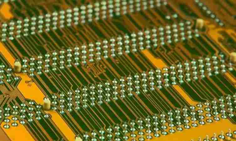
In addition, the packaging type and installation type of the terminal matching resistor must also be considered. Generally, SMD surface mount resistors have lower inductance than through-hole components, so SMD packaged components are preferred. If you choose a common in-line resistor, you can install it in two modes: vertical mode and horizontal mode.
In vertical installation, a short pin of the resistance can reduce the thermal resistance between the resistance and the circuit board, making it easier for the resistance heat to escape into the air. But a longer vertical installation will increase the resistance of the inductance. Horizontal installation has lower inductance due to lower installation. However, the overheated resistance will drift, and in the worst case, the resistance will become open circuit, resulting in the PCB end-of-line matching failure, which becomes a potential failure factor.
1. Methods to suppress electromagnetic interference
The electromagnetic compatibility (EMC) of PCB board can be improved by solving signal integrity problem well. It is very important to ensure that the PCB board is well grounded. It is very effective to adopt one signal layer and one ground layer for complex design. In addition, minimizing the density of the outermost signal on the circuit board is also a good way to reduce electromagnetic radiation. This method can be achieved by using "surface area layer" technology "Build-up" design of PCB. The surface area layer is achieved by adding a combination of thin insulation layers to the ordinary process PCB and micropores used to penetrate these layers. The resistance and capacitance can be buried under the surface layer, and the linear density per unit area can be nearly doubled, thus reducing the size of the PCB. The reduction of PCB area has a huge effect on the topology of the circuit, which means that the reduced current loop, the reduced branch length, and the electromagnetic radiation is approximately proportional to the area of the current loop; At the same time, the small size means that high density pin packages can be used, which in turn reduces the wire length, thus reducing the current loop and improving EMC characteristics.
2. Other technologies may be used
In order to reduce the voltage transient overshoot on the power supply of the IC chip, the decoupling capacitor should be added to the IC chip. This effectively removes the effect of burrs on the power supply and reduces the radiation from the power loop on the printed board.
The decoupling capacitor is best smoothed when it is connected directly to the power leg of the integrated circuit rather than to the power layer. This is why some devices have decoupling capacitors in the socket, and some devices require the decoupling capacitors to be sufficiently small from the device.
Any high speed and high power devices should be placed together as far as possible to reduce the instantaneous supply voltage overshoot.
If there is no power layer, then the long power cable will form a loop between the signal and the loop, becoming a radiation source and inductive circuit.
Open loop when the cables form a loop that does not pass through the same network cable or other cables. If the loop passes through the same network cable, other wires form a closed loop. In both cases, an antenna effect (wire antenna and ring antenna) occurs. The antenna produces EMI radiation externally and is itself a sensitive circuit. The closed loop is a problem that must be considered because the radiation it produces is approximately proportional to the area of the closed loop.

High-speed circuit design is a very complex design process. ZUKEN's high-speed circuit routing algorithm (Route Editor) and EMC/EMI analysis software (INCASES,Hot-Stage) are applied to analyze and find problems. The method described in this paper is designed to solve these problems of high speed circuit design. In addition, there are several factors that need to be considered in the design of high-speed circuits, and these factors are sometimes opposed to each other. For example, when high-speed devices are arranged close to each other, although the delay can be reduced, crosstalk and significant thermal effects may occur. Therefore, in the design, need to weigh each factor, make a comprehensive compromise consideration; Not only meet the design requirements, but also reduce the design complexity. The adoption of high speed PCB design means constitutes the controllability of the design process, only controllable, is reliable, can also be successful!
The circuit board on which the PCB is based
Feb 07,2023


Just upload Gerber files, BOM files and design files, and the KINGFORD team will provide a complete quotation within 24h.