
Professional PCB manufacturing and assembly
Building 6, Zone 3, Yuekang Road,Bao'an District, Shenzhen, China
+86-13410863085Mon.-Sat.08:00-20:00

A, decoupling capacitor configuration
In DC power supply loop, load variation can cause power supply noise. In a digital circuit, for example, a large spike of current is generated along the power line when the circuit changes from one state to another, creating a transient noise voltage. The configuration of decoupling capacitance can suppress the noise caused by load changes, which is a common practice in the reliability design of printed circuit boards. The configuration principle is as follows:
● The input end of the power supply is connected to a 10 ~ 100uF electrolytic capacitor. If the position of the printed circuit board allows, the anti-interference effect of the electrolytic capacitor above 100uF will be better.
● Configure a 0.01uF ceramic capacitor for each IC chip. If the printed circuit board space is too small to fit, a 1 ~ 10uF tantalum electrolytic capacitor can be configured for every 4 ~ 10 chips. The high frequency impedance of this device is very small, the impedance is less than 1Ω in the range of 500kHz ~ 20MHz, and the leakage current is very small (less than 0.5uA).
● For devices with weak noise capacity and large current change when off and memory devices such as ROM and RAM, the decoupling capacitor should be directly connected between the power line (Vcc) and ground (GND) of the chip.
● The lead of the decoupling capacitor should not be too long, especially the high-frequency bypass capacitor should not have a lead.
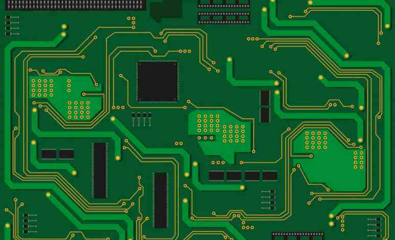
Two, printed circuit board size and device layout
Printed circuit board size should be moderate, too large printed line long, impedance increase, not only noise resistance decreases, the cost is high; Too small, the heat dissipation is not good, and easy to be disturbed by nearby lines.
As with other logic circuits, the device layout should be put as close to each other as possible, so that better anti-noise effect can be obtained. As shown in Figure 2. Time generator, crystal oscillator and CPU clock input are easy to produce noise, to be closer to each other. It is very important that noisy devices, small current circuits, large current circuits, etc. should be kept away from logic circuits as far as possible. If possible, circuit boards should be made separately

Three, thermal design
From the point of view that is conducive to heat dissipation, the printing plate is best installed upright, the distance between the plate and the plate should not be less than 2cm, and the arrangement of devices on the printing plate should follow certain rules:
· For devices with free convection air cooling, it is preferable to arrange integrated circuits (or other devices) in a longitudinal manner, as shown in Figure 3; For devices that use forced air cooling, it is preferable to arrange integrated circuits (or other devices) in a horizontal way, as shown in Figure 4.
· Devices on the same printed board should be arranged according to their calorific value and heat dissipation degree as far as possible. Devices with small calorific value or poor heat resistance (such as small signal transistors, small-scale integrated circuits, electrolytic capacitors, etc.) should be placed at the upper stream (entrance) of the cooling flow. Devices with high calorific value or good heat resistance (such as power transistors, large-scale integrated circuits, etc.) are placed at the downstream of the cooling flow.
· In the horizontal direction, the high-power devices should be arranged as close to the edge of the printed board as possible to shorten the heat transfer path; In the vertical direction, the high-power components are arranged as close as possible to the top of the printed board, so as to reduce the influence of these components on the temperature of other components.
· Devices sensitive to temperature should be placed in the area with the lowest temperature (such as the bottom of the device), and should not be placed directly above the heating device. Multiple devices should be staggered on a horizontal plane.
· The heat dissipation of the printed board in the equipment mainly depends on the air flow, so the air flow path should be studied during the design, and the device or printed circuit board should be reasonably configured. Air flow always tends to flow where the resistance is low, so when configuring components on the printed circuit board, avoid leaving a large area of airspace. The configuration of multiple printed circuit boards in the whole machine should also pay attention to the same problem.
A lot of practical experience shows that the temperature rise of printed circuit can be reduced effectively by adopting a reasonable arrangement of devices, so that the failure rate of devices and equipment can be significantly reduced.
The above mentioned are just some general principles of reliability design of printed circuit board. The reliability of printed circuit board is closely related to the specific circuit. In order to ensure the reliability of printed circuit board to the maximum extent, it is not necessary to carry out corresponding processing according to the specific circuit in the design.
Fourth, product harassment suppression program
1 Grounding 1.1 Grounding signals of the device
Purpose: To provide a common reference potential for any signal in the device.
Mode: The signal grounding system of the device can be a metal plate.
1.2 Basic Signal grounding Methods
There are three basic signal grounding modes: floating ground, single point ground, and multi-point ground.
1.2.1 Floating ground purpose: to isolate the circuit or equipment from the common wire that may cause circulation due to the common ground wire. Floating ground also makes it easy to cooperate between circuits with different potentials. Disadvantages: electrostatic accumulation is easy to cause strong electrostatic discharge. Compromise: Access the bleed resistor.
1.2.2 Single-point grounding: Only one physical point in a line is defined as a grounding reference point. All grounding points need to be connected to this point. Disadvantages: Not suitable for high frequency applications.
1.2.3 Multi-point grounding: The point that needs to be grounded should be directly connected to the ground plane nearest to it so that the length of the grounding cable is the shortest. Cons: More cumbersome to maintain.
1.2.4 Hybrid grounding Single point and multi-point grounding should be selected as required.
1.3 Processing of signal Ground Wires (lapping)
A bond is a path of low impedance between two metal points.
Direct lap joint and indirect lap joint.
No matter what kind of lap, the most important thing is to emphasize good lap.
1.4 Device Grounding (Grounding)
The equipment is connected to the earth, with the earth as the reference point, purpose:
1) Realize safe grounding of equipment
2) Release the accumulated charge on the chassis to avoid internal discharge of the equipment.
3) The working stability of the high equipment can avoid the change of the potential of the equipment to the earth under the action of the external electromagnetic environment.
1.5 Method of enlarging ground and grounding resistance grounding rod.
1.6 Grounding electrical equipment
PCB shield
Feb 06,2023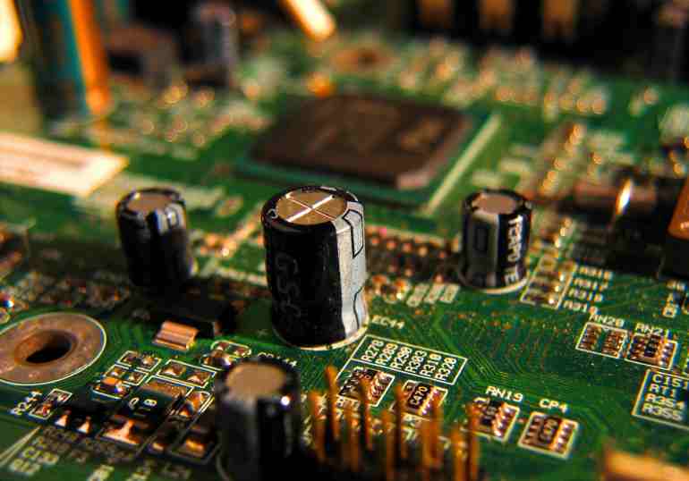


Just upload Gerber files, BOM files and design files, and the KINGFORD team will provide a complete quotation within 24h.