
Professional PCB manufacturing and assembly
Building 6, Zone 3, Yuekang Road,Bao'an District, Shenzhen, China
+86-13410863085Mon.-Sat.08:00-20:00

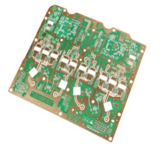
Storage and shelf life of PCB production requirements for high-frequency PCB
PCB manufacturers, PCB designers and PCBA processors explain the storage and shelf life requirements for high-frequency PCB production
After the final finished product inspection, PCB boards are vacuum packed and stored for shipment. Then why do PCB boards need vacuum packaging? How to store after vacuum packaging? How long is its shelf life? The following circuit board factory will briefly introduce the storage mode and shelf life of PCB.
Why do PCB boards need vacuum packaging? Although this problem is small, many circuit board manufacturers attach great importance to it. Because once the PCB board is not sealed well, its surface gold deposition, tin spraying and bonding pad parts will be oxidized and affect welding, which is not conducive to production.
How do I store PCB boards? The circuit board is not in contact with air and water as other products. First of all, the vacuum of PCB board cannot be damaged. When packing, a layer of bubble film needs to be enclosed on the side of the box. The bubble film has good water absorption, which plays a good role in moisture-proof. Of course, moisture-proof beads are also indispensable. Then classify and discharge them and label them. After sealing, the box must be stored in a dry and ventilated place separated from the wall and away from the ground, and also protected from sunlight. The temperature of the warehouse should be better controlled at 23 ± 3 ℃ and 55 ± 10% RH. Under such conditions, PCB boards with surface treatment such as gold deposition, electrowinning, tin spraying and silver plating can be stored for 6 months, and PCB boards with surface treatment such as silver deposition, tin deposition and OSP can be stored for 3 months.
For PCB boards that have not been used for a long time, the circuit board manufacturer should brush a layer of three proof paint on them, which can prevent moisture, dust and oxidation. In this way, the storage life of PCB will be increased to 9 months.
What are the specific requirements for high-frequency PCB production?
High frequency board refers to special circuit board with high electromagnetic frequency. Generally speaking, high frequency can be defined as frequency above 1GHz. High frequency circuit board has a wide range of applications, and has strict requirements in design and manufacturing. What are the specific requirements for high-frequency PCB production?
1. 45 ° angle shall be adopted for transmission line corner to reduce return loss;
2. The high-performance dielectric circuit board whose dielectric constant is strictly controlled according to the number of layers is used. This method is conducive to the effective simulation of the electromagnetic field between the insulating material and the adjacent wiring.
3. It is produced according to the PCB design specifications for high-precision etching. The total error of wire width is specified to be+/-0.0007 inches. It is very important to manage the geometry of wiring (wire) and coating surface as a whole to solve the skin effect problem related to microwave frequency and realize these specifications.
4. In high-frequency environment, it is better to use surface mounted SMD components and avoid using components with leads.
5. For signal vias, avoid using the through hole machining (pth) process on the sensitive plate, because this process will cause lead inductance at the vias; The blind hole or back drill shall be used.
6. Rich grounding layers shall be provided to prevent the influence of three-dimensional electromagnetic field on the circuit board.
7. The non electrolytic nickel plating or gold immersion plating process shall be selected, and the HASL method shall not be used for electroplating; This electroplating can provide better skin effect for high-frequency current and help reduce environmental pollution.
8. The solder barrier layer can prevent the flow of solder paste. Generally, the solder dam is used as the solder barrier layer. PCB manufacturers, PCB designers and PCBA manufacturers explain the storage and shelf life requirements of high-frequency PCB boards.


Just upload Gerber files, BOM files and design files, and the KINGFORD team will provide a complete quotation within 24h.