
Professional PCB manufacturing and assembly
Building 6, Zone 3, Yuekang Road,Bao'an District, Shenzhen, China
+86-13410863085Mon.-Sat.08:00-20:00

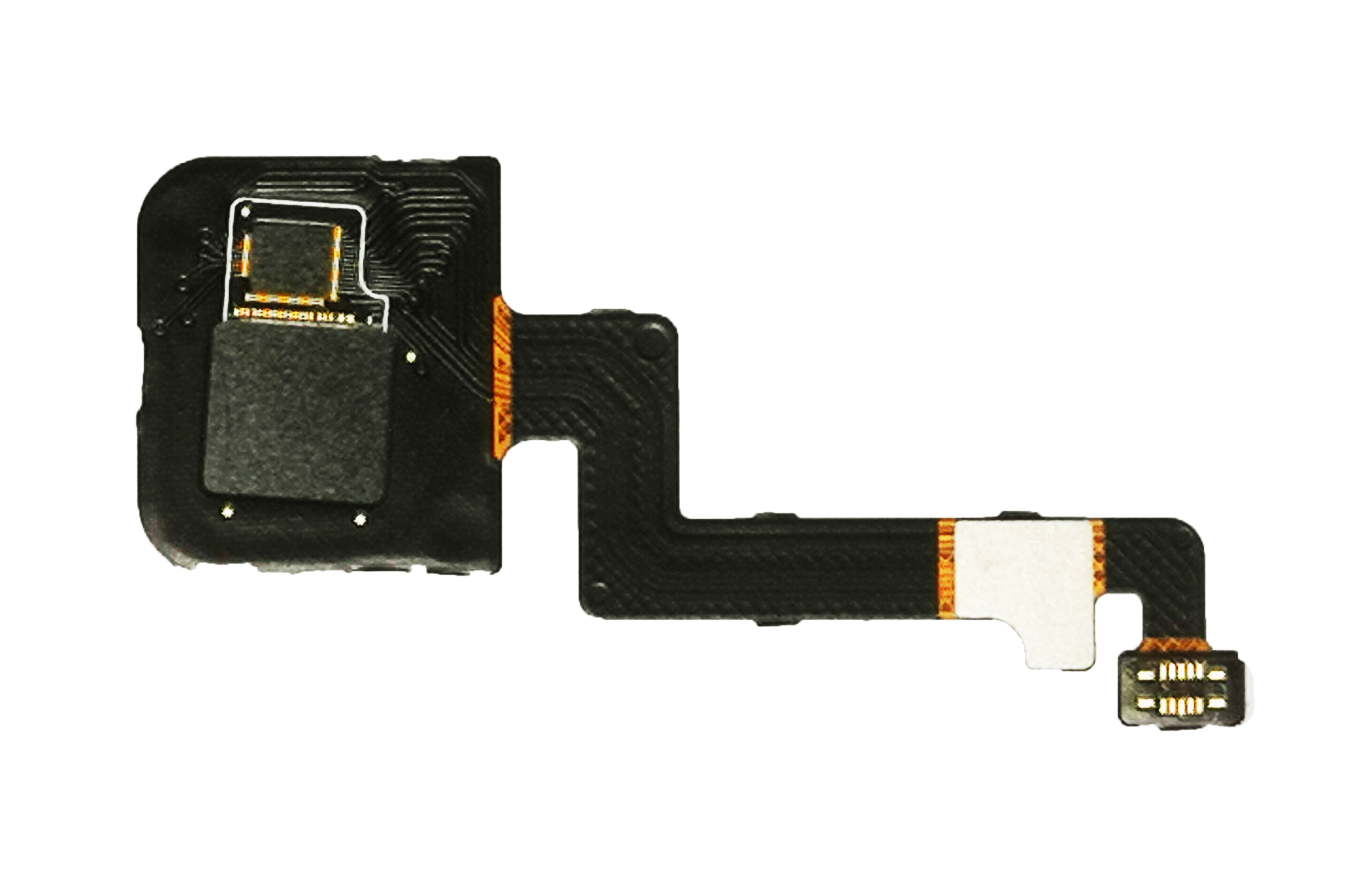
Process of Soldering Resistance Layer for Flexible Circuit Board PCB
PCB manufacturing, PCB design and PCBA processing manufacturers will explain the process of solder mask of FPC PCB
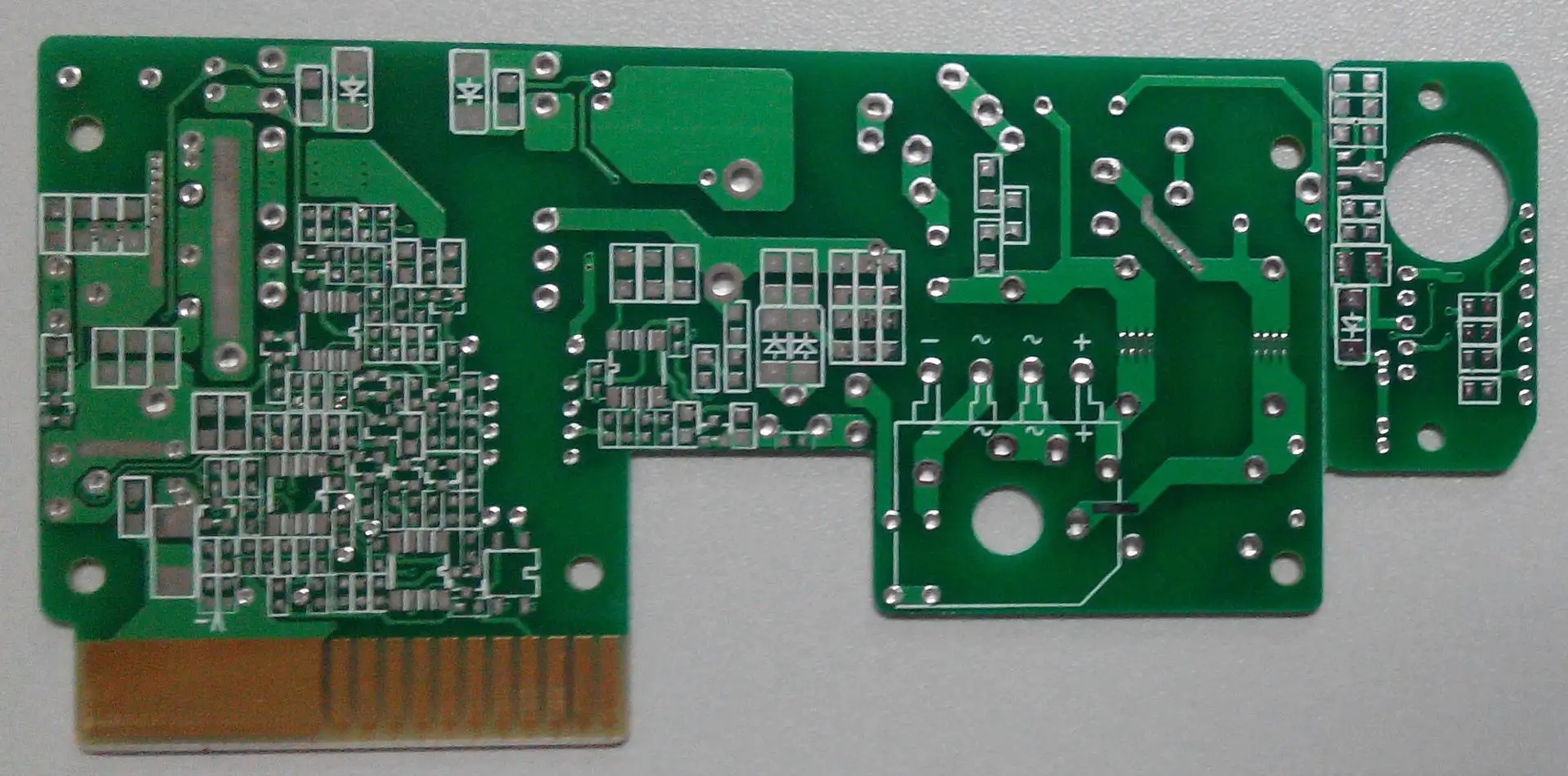
The PCB we see in our daily life is basically composed of solder mask, silk screen layer, copper wire and other parts. Generally speaking, we call the part on the flexible circuit board that needs green oil solder mask; The solder mask uses negative output, so after the shape of the solder mask is mapped to the board, the solder mask is not covered with green oil, but exposed with copper. The role of the solder mask in controlling the reflow process is very important.
The soldering process in FPC is to screen print printed boards with soldering resistance. The solder pad on the printed board is covered with a photographic plate so that it is not exposed to ultraviolet radiation. The solder mask is more firmly attached to the printed board surface after ultraviolet radiation. The solder pad is not exposed to ultraviolet radiation, and the copper solder pad can be exposed, so that lead tin can be applied during hot air leveling. Today's FPC editor wants to focus on the process of solder mask.
1. Prebake
The purpose of pre drying is to evaporate the solvent contained in the ink and make the solder mask non stick. For different inks, the pre drying temperature and time are different. Too high pre baking temperature or too long drying time will lead to poor development and reduce the resolution; If the pre drying time is too short or the temperature is too low, the negative film will stick when exposed. When developing, the solder mask will be eroded by sodium carbonate solution, causing the surface to lose luster or the solder mask to expand and fall off.
2. Exposure
Exposure is the key to the whole process. If the exposure is excessive, due to light scattering, the solder mask at the edge of the pattern or line reacts with the light (mainly the photosensitive polymer contained in the solder mask reacts with the light) to generate a residual film, which reduces the resolution, resulting in smaller developed patterns and thinner lines; If the exposure is insufficient, the result is contrary to the above, and the developed figure becomes larger and the lines become thicker. This situation can be reflected by the test: if the exposure time is long, the measured line width is negative tolerance; If the exposure time is short, the measured line width is a positive tolerance. In the actual process, the "light energy integrator" can be selected to determine the optimal exposure time.
3. Ink viscosity adjustment
The viscosity of liquid photosensitive solder resist ink is mainly controlled by the ratio of hardener and main agent and the addition amount of thinner. If the addition of hardener is not enough, it may cause imbalance of ink characteristics. PCB manufacturing, PCB design and PCBA processing manufacturers will explain the process of solder mask of FPC PCB.


Just upload Gerber files, BOM files and design files, and the KINGFORD team will provide a complete quotation within 24h.