
Professional PCB manufacturing and assembly
Building 6, Zone 3, Yuekang Road,Bao'an District, Shenzhen, China
+86-13410863085Mon.-Sat.08:00-20:00

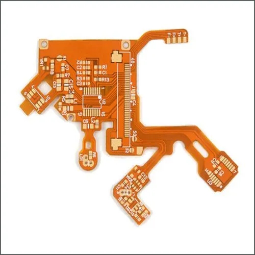
Characteristics of PCB surface gold deposition process and placement of capacitors
PCB manufacturing, PCB design and PCBA processing manufacturers will explain the characteristics of PCB surface treatment and the placement of capacitors
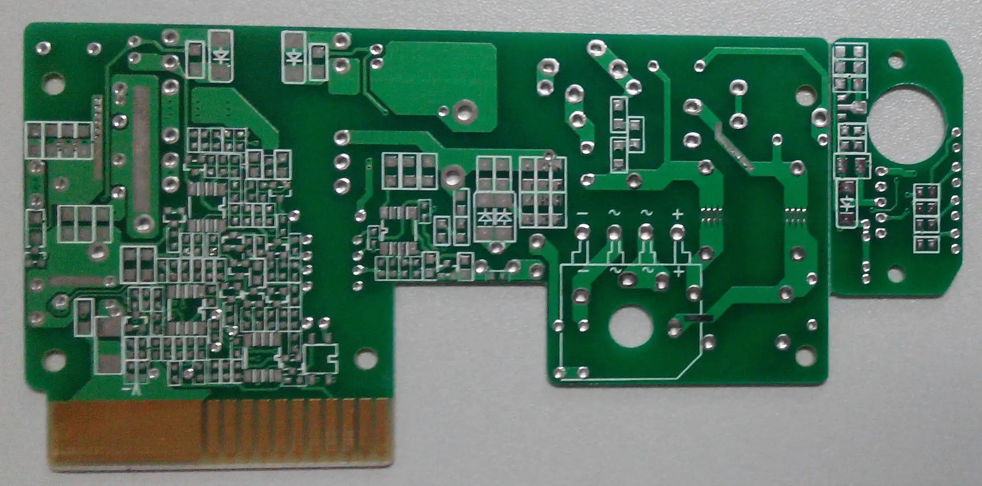
How important are circuit boards in our lives? For us, almost everyone will contact with the circuit board every day, such as various electrical appliances and electronic products. However, a PCB must go through a variety of manufacturing processes to complete the process. Now, let's focus on the gilding process of PCB surface.
In the surface treatment of PCB, there is a very common process called gilding. Gold deposition process is to deposit nickel gold coating with stable color, good brightness, flat coating and good solderability on the surface of PCB printed circuit.
In addition, after gilding, PCB presents a golden yellow color, which is more golden than the color of gilding, because it is more bright and beautiful after gilding, which is the saying that good appearance can sell at a good price. For our customers, what is presented to customers is high quality, looks very comfortable, and customers will be more satisfied with our products;
Therefore, I summarized its characteristics as follows:
1. The gilt plate is bright in color, good in color and good in appearance, which improves the attractiveness to customers.
2. The crystal structure formed by gold precipitation is easier to weld than other surface treatments, which can have better performance and ensure quality.
3. As the gold plate only has nickel gold on the pad, it will not affect the signal, because the signal transmission in skin effect is in the copper layer.
4. Since only the bonding pad of the gold plated plate has nickel gold, the bonding between the resistance solder and the copper layer on the circuit is stronger, and it is not easy to cause micro short circuit.
5. The project will not affect the spacing during compensation, which is convenient for work.
Most manufacturers will receive complaints from customers about poor welding due to the lack of gilding treatment. At the same time, because the gilding is softer than the gilding, the gilding plate is not wear-resistant. The flatness and standby life of PCB gilt plate are as good as that of gilt plate, so at present, most factories adopt the gilt process to produce gold plate.
Have you placed the car circuit board and capacitor correctly?
The power supply chip is indispensable to the automobile circuit board. We usually use a large capacitor (100 microf to 1000 microf) and a small capacitor (0.1 microf or 0.01 microf) as the filter capacitor of the power supply.
Large capacitors are used to filter low frequency noise, while small capacitors are used to filter high frequency noise.
You have designed so many automobile circuit boards. Have you placed the capacitors on the automobile circuit boards correctly?
After the positive pole of the power supply comes in, whether the capacitance is too large or small first. The correct connection method is: first too large capacitance, then too small capacitance.
In general, which connection method can be used. In high-precision applications, in order to minimize the noise of the power supply, it is best to connect according to the correct method described above, with the best filtering effect. PCB manufacturers, PCB designers and PCBA processors will explain the characteristics of the PCB surface treatment gold deposition process and the placement of capacitors.


Just upload Gerber files, BOM files and design files, and the KINGFORD team will provide a complete quotation within 24h.