
Professional PCB manufacturing and assembly
Building 6, Zone 3, Yuekang Road,Bao'an District, Shenzhen, China
+86-13410863085Mon.-Sat.08:00-20:00

Overview of etching process for outer circuit of high frequency board
Circuit board manufacturing, circuit board design, PCBA processing manufacturer will explain the etching process overview of the outer circuit of high-frequency board
1、 Overview
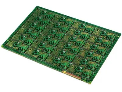
At present, the typical processing technology of printed circuit board (PCB high-frequency board/Rogers high-frequency mixed plate) is "graphic electroplating". That is to say, a layer of lead tin anti-corrosive coating is pre coated on the copper foil part to be reserved on the outer layer of the board, that is, the graphic part of the circuit, and then the rest of the copper foil is chemically etched, which is called etching.
It should be noted that there are two layers of copper on the PCB high-frequency board/Logers high-frequency composite board In the outer layer etching process, only one layer of copper must be completely etched, and the rest will form the final required circuit. This type of pattern electroplating is characterized by that the copper plating layer only exists below the lead tin corrosion resistant layer. Another process method is that the entire PCB high frequency board/Rogers high frequency composite board is coated with copper, and the parts other than the photosensitive film are only tin or lead tin corrosion resistant layers. This process is called "full board copper plating process". Compared with graphic electroplating, the biggest disadvantage of full board copper plating is that the PCB high-frequency board/Logers high-frequency mixed board must be plated with copper twice everywhere and must be corroded during etching. Therefore, when the wire width is very fine, a series of problems will occur. At the same time, side corrosion will seriously affect the uniformity of the line.
In the processing technology of the outer circuit of the PCB high-frequency board/Logers high-frequency hybrid board, another method is to use a photosensitive film to replace the metal coating as the anti-corrosion layer. This method is very similar to the inner layer etching process. Please refer to the etching in the inner layer fabrication process.
At present, tin or lead tin is the most commonly used anti-corrosion layer, which is used in the etching process of ammonia etchant Ammonia etchant is a commonly used chemical solution, which does not have any chemical reaction with tin or lead tin. Ammonia etchant mainly refers to ammonia/ammonia chloride etchant. In addition, ammonia/ammonia sulfate etching solution can also be purchased in the market.
After use, the copper in the sulfate based etching solution can be separated by electrolysis, so it can be reused. Because of its low corrosion rate, it is rarely seen in actual production, but it is expected to be used in chlorine free etching. Someone tried to use sulfuric acid hydrogen peroxide as an etchant to etch the outer figure. For many reasons, including economy and waste liquid treatment, this process has not been widely used in commercial sense Furthermore, sulfuric acid hydrogen peroxide cannot be used for etching the lead tin corrosion resistant layer, and this process is not the main method for making the outer layer of PCB high-frequency board/Logers high-frequency composite board, so most people rarely pay attention to it.
Circuit board manufacturing, circuit board design and PCBA processing manufacturers will give you an overview of the etching process for the outer circuit of high-frequency boards.


Just upload Gerber files, BOM files and design files, and the KINGFORD team will provide a complete quotation within 24h.