
Professional PCB manufacturing and assembly
Building 6, Zone 3, Yuekang Road,Bao'an District, Shenzhen, China
+86-13410863085Mon.-Sat.08:00-20:00

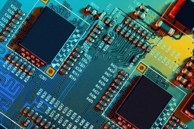
Introduction to the causes and elimination of failures in the nickel plating process of PCB
The circuit board manufacturer, circuit board designer and PCBA processor explain the causes and troubleshooting of the failures in the circuit board nickel plating procedure
a) Ma Hang: Ma Hang is the result of organic pollution. Large pits usually indicate oil pollution. If the mixing is not good, the bubbles cannot be expelled, which will form pockmarks. Wetting agent can be used to reduce its impact. We usually call small pits pinholes. Pinholes can be generated due to poor pretreatment, metal impurities, too little boric acid content, and too low bath temperature. Bath maintenance and process control are the keys. Anti pinhole agent should be used as process stabilizer to supplement.
b) Roughness and burr: Roughness indicates that the solution is dirty, which can be corrected by adequate filtration (too high PH is easy to form
The precipitation of hydroxide should be controlled). If the current density is too high, impurities are brought into the anode mud and impure added water, which will cause roughness and burrs in serious cases.
c) Low adhesion: if the copper coating is not fully oxidized, the coating will peel off, and the adhesion between copper and nickel is poor. If the current is interrupted, the nickel coating will peel off at the interruption point, and it will also peel off when the temperature is too low and serious.
d) Brittleness and poor solderability of the coating: when the coating is bent or worn to some extent, the coating brittleness is usually exposed. This indicates that there is organic matter or heavy metal pollution. Excessive additives, entrained organic matter and electroplating corrosion inhibitor are the main sources of organic matter pollution, which must be treated with activated carbon. Insufficient additives and high PH will also affect the brittleness of the coating.
e) Coating darkening and uneven color: coating darkening and uneven color indicate metal pollution. Since copper plating is generally followed by nickel plating, the copper solution brought in is the main pollution source. It is important to minimize the copper solution on the hanger. In order to remove the metal pollution in the tank, especially the copper removal solution, the corrugated steel cathode should be used. Under the current density of 2~5 A/square foot, 5 amperes per gallon of solution should be empty plated for one hour. Poor pretreatment, poor low coating, too low current density, too low concentration of main salt, and poor contact of electroplating power circuit will affect the coating color.
f) Coating burn: Possible causes of coating burn: insufficient boric acid, low concentration of metal salt, low working temperature, high current density, high PH or insufficient stirring.
g) Low deposition rate: low pH value or low current density will cause low deposition rate.
h) Blistering or peeling of the coating: blistering or peeling will occur in case of poor pre-treatment, too long interruption time, organic impurity pollution, too high current density, too low temperature, too high or too low PH, and serious influence of impurities.
1) Anode passivation: the anode activator is insufficient, the anode area is too small, and the current density is too high.
Process Instructions for Liquid Photosensitive Exposure and Development
I Objective: This instruction specifies the work contents and steps of the PCB positioning exposure production station after the drying of the liquid photosensitive ink screen printing.
II Scope: This instruction is applicable to the exposure station production of double-sided board, multilayer board and single panel with silk screen liquid ink.
3、 Equipment:
Exposure machine
4、 Material:
Diazo working film
Alcohol (industrial use)
adhesive tape
Printed circuit board pre dried with liquid ink
5、 Process steps:
5.1 Exposure positioning:
During the first exposure, use a magnifying glass to check the positioning accuracy of the PCB board before exposure after vacuuming. If there is any deviation, correct it in time.
5.1.1 Position the self inspection film before exposure, check the correctness of the film according to the construction sheet, and check each batch of films for positioning. If there is any error, correct the PCB board in time and handle it gently to prevent the film from being scratched.
5.2 Starting the exposure machine
Open the main power switch and the chilled water valve.
Turn on the startup switch of the exposure machine, check and turn on the emergency switch.
Enter the interface and press System Start.
Check all parameters and enter manual mode. Turn on the exposure lamp switch. Wait 15 minutes before exposure to ensure that the exposure lamp is fully warmed up.
Enter automatic state
Check that the exposure index is set to the correct value.
start-up
5.3 Clean the frame glass and polyester film.
Open the frame, put in the positioned PCB, and put down the frame to lock it.
Press the vacuum switch, and the machine will automatically expose.
Open the frame, take out the exposed PCB, place the positioned PCB, and put down the frame to lock it.
Repeat steps 5.3.2 - 5.3.4
5.4 Turn off the exposure machine
Turn off the exposure lamp switch manually, wait 15 minutes, and then turn off the system.
Turn off the main power switch.
Close the cooling water valve.
5.4.4 After exposure, the circuit board shall not be placed for more than 24 hours at most.
5.5 Precautions:
Clean the exposure frame frequently with alcohol.
When exposing the circuit board, handle it gently to avoid scratching the working negative.
The vacuum degree requires that the displayed value of the vacuum gauge is greater than 700.
Before exposure, it must be noted that the PCB board should be fully cooled and the board surface should not stick to the negative film.
Before positioning, check whether the model of the construction ticket is consistent with the negative film.
5.6 After the construction is completed, the Construction Permit, Scrap Sheet and Rework Sheet must be carefully filled in.
6、 Security:
Take care not to expose the ultraviolet light of the exposure machine.
When the UV lamp is turned on, the machine shell must not be opened.
7、 Relevant record forms:<construction order>,<rework order>,<scrap order>.
Section II Liquid Photosensitive Development Process
I Objective: This instruction specifies the work contents and steps of the development and production station of exposed liquid photosensitive circuit boards.
2、 Scope: This instruction is applicable to the working process of the development and production station.
3、 Equipment:
UNIVERS Developer
4、 Material:
sodium carbonate
Defoamer
Water softening
Printed board coated with liquid photosensitive ink for complete exposure
5、 Process:
5.1 Operation steps
Before startup:
Before starting the equipment, it must be checked that the whole equipment and its outer cover are tightly closed and the exhaust pipe valve is open.
Clean all nozzles and flush water tanks daily.
Clean the drying roller and the machine in the drying section.
Clean and replace the circulating water washing tank every day.
5.1.1 Close all covers on the machine, otherwise the developer cannot be started.
5.1.2 Opening:
Main power switch check emergency switch
Developer spray pump switch
Developing part spray moving switch
Water wash switch after development
Drying system switch
5.2 Operating parameters:
Developer temperature: 28 - 34 degrees
Developer concentration: sodium carbonate 0.8 - 1.05%
Developing moving speed: 1.0-1.4M/mIN
Developing pressure 2.2-2.6 BAR
Water washing pressure 4.0-4.5 BAR
5.3 Solution replacement and preparation:
5.3.1 1% sodium carbonate solution: change every day
The tank volume is 400L. 4KG anhydrous sodium carbonate shall be added to prepare 1% sodium carbonate solution. After dissolution, softened water shall be filled, and 1L defoamer shall be added. After the solution is prepared, it shall be stirred and circulated for half an hour, and the analysis room shall be notified for testing before use.
5.4 After the construction is completed, the "construction ticket", "scrap sheet" and "rework sheet" must be carefully filled in.
6、 Self inspection:
After the development of the outer panel, the bonding pad must be complete without residual ink.
The solder mask surface is clean without color difference, and the graphics are complete without scratches.
After development, the PCB board is free of over development, ghost and other phenomena.
7、 Security:
The operator must wash his hands after handling the developing solution.
After contacting the developing solution, the body part should be cleaned with water immediately. If your eyes are splashed with developer solution, wash them with water immediately and see a doctor.
VIII Record forms:<Analysis form ANALYSIS OF DEVELOPMENT>,<Construction ticket>,<Scrap sheet>,<Rework sheet>. The circuit board manufacturer, circuit board designer and PCBA processor will explain the causes and troubleshooting of the failures in the circuit board nickel plating process.


Just upload Gerber files, BOM files and design files, and the KINGFORD team will provide a complete quotation within 24h.