
Professional PCB manufacturing and assembly
Building 6, Zone 3, Yuekang Road,Bao'an District, Shenzhen, China
+86-13410863085Mon.-Sat.08:00-20:00

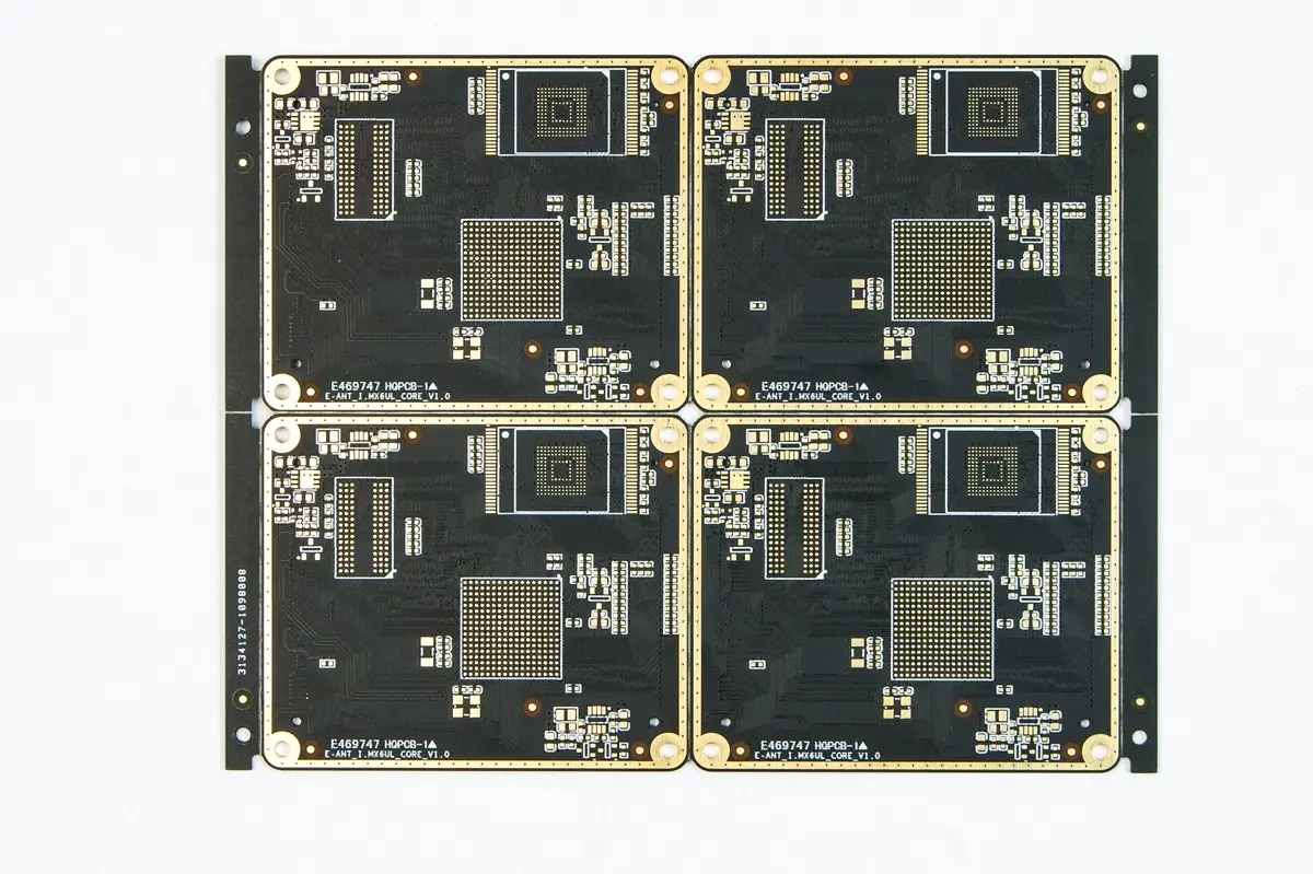
Detailed explanation of high-precision 8-layer PCB production
Circuit board manufacturing, circuit board design and PCBA processing manufacturers explain the details of high-precision 8-layer circuit board manufacturing
High precision eight layer circuit board is now one of the mainstream finished products in printed circuit boards. Because its wiring density is much higher than that of single-sided PCB circuit board, and electronic components can be installed on both sides, making the structure of electronic products more reasonable, it quickly replaced single-sided circuit board once it appeared, and became a basic unit product developing towards PCB multilayer boards. The process is mature and the technology is more complex. Eight layer PCB can provide high-efficiency and high-quality single-sided PCB, double-sided PCB and high-precision eight layer PCB manufacturers.
Wiring method of 8-layer circuit board:
Generally speaking, eight layer pcb circuit board can be divided into top layer, bottom layer and two middle layers. The top layer and the bottom layer run signal lines. The middle layer first uses the command DESIGN/LAYERSTACKMANAGER to add INTERNALPLANE1 and INTERNALPLANE2 as multiple power layers, such as VCC, and layers, such as GND, respectively (that is, connect the corresponding network labels. (Note that ADDLAYER is not used, which will increase MIDPLAYER, which is mainly used to place multi-layer signal lines). In this way, PLNNE1 and PLANE2 are copper sheets connecting the two layers of power VCC and GND.
If the copper sheet is not flattened, it will wrinkle. The thinner the copper sheet is used as the pressing plate of PCB multilayer board, the higher the crease chance. The thicker the copper sheet, the lower the crease chance. If it is confirmed that the copper sheet is flat during operation, it depends on whether it is the blank area of the base material. If the film produces a large amount of flow in the melting process, the possibility of sliding due to poor support of the copper sheet will occur. Therefore, most circuit board manufacturers will pay attention to the circuit configuration problem of the inner substrate, and try to avoid making the empty area too obvious. Most copper wrinkling occurs in areas with large difference in line density, especially in areas where one side is designed as a large copper surface and the other side is designed as a large empty area.
In addition, film (PP) combination and hot pressing parameters are also very important. If the film overlaps and moves or the glue flow is improper, the copper sheet will float on the surface of the melt resin, which will inevitably cause wrinkles. To prevent such problems, the carrier plate used for pressing plate is the key point of operation. At present, most of the tray designs used by the industry have adopted the sliding prevention design with elastic height regulation, which can completely prevent the steel plate from slipping during the pressing process, so that the crease will not occur.
In terms of film selection, the type with too high glue content shall not be used as far as possible, and the pressing temperature rise rate shall also be at a lower level, as long as the filling is complete. If the PCB produced already has wrinkles, in the case of loose product specifications, it can be considered to remove the surface copper and make a new press fit. Although the plate thickness will be slightly higher, it can still be remedied if the customer specifications are acceptable.
Let's share the processing flow of high-precision 8-layer circuit board:
Blanking of eight layer copper clad plate, drilling of reference hole, CNC drilling of through hole, inspection, deburring, brushing, chemical plating (through hole metallization), electroplating of thin copper on the whole plate, inspection, brushing, screen printing of negative circuit graphics, curing (dry film or wet film, exposure, development), inspection Repair - circuit pattern electroplating - electrotinning (corrosion resistant nickel/gold) - printing material removal (photosensitive film) - etching copper - tin removal - cleaning and brushing - screen printing solder resistance pattern (pasting photosensitive dry film or wet film, exposure, development, thermal curing, commonly used photosensitive and thermal curing green oil) - cleaning, drying - screen printing marking characters and patterns, curing - contour processing, cleaning, drying - electrical on/off detection - tin spraying or organic solder protection film - inspection, packaging and delivery of finished products.
Above the eighth floor, there are through holes and blind holes. Through holes are drilled from the top floor to the bottom floor, while blind holes can only be seen on one of the top floor or the bottom floor. The other floor is invisible. That is to say, blind holes are drilled from the surface, but they do not penetrate all layers. Another kind is called buried hole. The buried hole refers to the hole made in the inner layer, and the surface and bottom layers are invisible. The advantage of making buried holes and blind holes is to increase the wiring space. Circuit board manufacturing, circuit board design and PCBA processing manufacturers will explain the production of high-precision 8-layer circuit boards in detail.


Just upload Gerber files, BOM files and design files, and the KINGFORD team will provide a complete quotation within 24h.