
Professional PCB manufacturing and assembly
Building 6, Zone 3, Yuekang Road,Bao'an District, Shenzhen, China
+86-13410863085Mon.-Sat.08:00-20:00

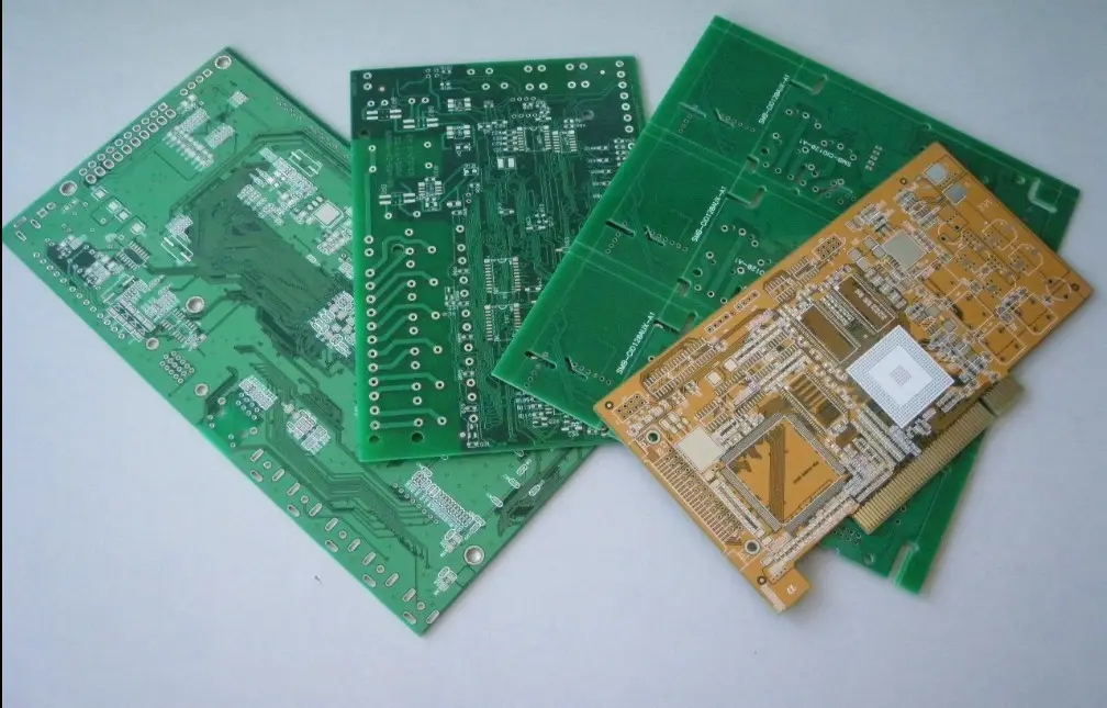
PCB manufacturer explains PCB design, PCB modification and PCB copy
In addition to the simple concept of copying the circuit board, PCB copying also includes the technical concepts of decryption of some encrypted chips on the board, reverse deduction of PCB schematic diagram, production of BOM list, PCB design, etc.
Backward deduction of PCB schematic diagram
Schematic diagram is a drawing composed of electrical symbols to analyze the circuit principle. It plays an indispensable role in the process of product debugging, maintenance and improvement. The reverse inference of schematic diagram is just the opposite of the forward design. The forward design is that the schematic diagram is designed first, and then the PCB is designed according to the schematic diagram. The reverse inference of schematic diagram of PCB refers to the reverse inference of the schematic diagram of the product according to the existing PCB file or PCB physical object, so as to facilitate the technical analysis of the product and assist in the later product prototype debugging, production or improvement and upgrading.
BOM list preparation
In the process of product reverse technology research and imitation development, the production of BOM list and placement orientation map, and the production of SMT placement machine component coordinate map are all necessary links for later template welding, placement processing, complete prototype finalization design and assembly production.
BOM (Bill of Materials) is the basis for component material procurement, which records various components, modules and other special materials required for product composition. The most important thing in the preparation of the BOM list is to require that the measured values of various parameters of components are accurate, because if the parameters of components are wrong, it may affect the accuracy of component judgment and material procurement, and even lead to project development failure.
PCB modification
PCB modification is a related concept in PCB copying. It refers to the circuit adjustment or re layout of the extracted PCB file to achieve the functional modification of the original circuit board, which can quickly update and upgrade the product to meet the personalized needs and special application needs of some customers.
PCB design
In high-speed design, the characteristic impedance of controllable impedance plate and circuit is one of the most important and common problems. First of all, let's understand the definition of transmission line: transmission line is composed of two conductors with a certain length. One conductor is used to send signals, and the other is used to receive signals (remember that the concept of "loop" replaces "ground"). In a multilayer board, each line is a part of the transmission line, and the adjacent reference plane can be used as the second line or loop. The key for a line to become a "good performance" transmission line is to keep its characteristic impedance constant throughout the line.
The key to becoming a "controllable impedance board" is to make the characteristic impedance of all circuits meet a specified value, usually between 25 ohms and 70 ohms. In multilayer circuit board, the key to good transmission linearity is to keep its characteristic impedance constant throughout the circuit.
But what is the characteristic impedance? The simplest way to understand the characteristic impedance is to see what the signal encounters during transmission. When moving along a transmission line with the same cross section, this is similar to the microwave transmission shown in Figure 1. Suppose that a 1-volt voltage step wave is added to this transmission line. For example, a 1-volt battery is connected to the front end of the transmission line (it is located between the transmission line and the loop). Once connected, this voltage wave signal travels along the line at the speed of light, and its speed is usually about 6 inches/nanosecond. Of course, this signal is really the voltage difference between the transmission line and the loop, which can be measured from any point of the transmission line and the adjacent point of the loop. Figure 2 is the transmission diagram of the voltage signal.
Zen's method is to "generate a signal" and then travel along this transmission line at a speed of 6 inches/nanosecond. The first 0.01 nanoseconds advance 0.06 inches. At this time, the sending line has redundant positive charges, while the loop has redundant negative charges. It is the difference between these two charges that maintains the 1 volt voltage difference between the two conductors, which in turn forms a capacitor.
In the next 0.01 nanosecond, adjust the voltage of a 0.06 inch transmission line from 0 to 1 volt. This requires adding some positive charges to the transmission line and some negative charges to the receiving line. For every 0.06 inch of movement, more positive charges must be added to the transmission line and more negative charges must be added to the circuit. Every 0.01 nanoseconds, another section of the transmission line must be charged, and then the signal begins to travel along this section. The charge comes from the battery at the front of the transmission line. When moving along this line, it charges the continuous part of the transmission line, thus forming a voltage difference of 1 volt between the transmission line and the loop. Every 0.01 nanoseconds forward, some charge (± Q) is obtained from the battery. The constant electric quantity (± Q) flowing from the battery within a constant time interval (± t) is a constant current. The negative current flowing into the loop is actually equal to the positive current flowing out, and it is just at the front end of the signal wave. The AC current passes through the capacitor composed of the upper and lower lines to end the whole cycle.
PCB manufacturers, PCB designers and PCBA manufacturers will explain PCB design, PCB modification and PCB copying.

How to judge the quality of PCB
Nov 10,2022


Just upload Gerber files, BOM files and design files, and the KINGFORD team will provide a complete quotation within 24h.