
Professional PCB manufacturing and assembly
Building 6, Zone 3, Yuekang Road,Bao'an District, Shenzhen, China
+86-13410863085Mon.-Sat.08:00-20:00

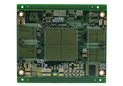
Do you know the copper plating process in PCB production of PCB factory
Today, I would like to share with you the PCB production process of the circuit board factory - copper sinking, which is a major process for the production of circuit boards in major circuit board factories. I will be responsible for explaining the copper sinking process today. Remember to listen carefully! Keep pace with Xiao Bian.
Copper plating is called through hole plating in the production process of circuit board factory, that is, electroless copper plating. In the PCB production process of Shenzhen Circuit Board Factory, the copper deposition process requires chemical reaction, usually abbreviated as PTH, which is a self catalyzed redox reaction. Generally, the double-sided board or multilayer board shall be copper plated after drilling.
The function of copper deposition is mainly to connect the circuit. On the base material of the wall of the non-conductive hole drilled, the chemical method - chemical copper is used, because there is also electroplated copper behind. The purpose of copper deposition is to make the base for the electroplated copper. Our Shenzhen Circuit Board Factory is very careful in the process flow of PCB production, and every step is carefully implemented.
The control of copper deposition process will affect some special PCB plates (such as PCB high-frequency plates, soft and hard bonding plates, thick copper plates, impedance plates, plate hole plates, thick gold plates, coil plates), and of course, it is more related to the quality of our products in Shenzhen Circuit Board Factory, so each process is strictly controlled.
Decomposition of copper precipitation process: alkaline degreasing → secondary or tertiary countercurrent rinsing → roughening (micro etching) → secondary countercurrent rinsing → pre leaching → activation → secondary countercurrent rinsing → degumming → secondary countercurrent rinsing → copper precipitation → secondary countercurrent rinsing → acid leaching
Of course, Xiao Bian will tell you more about the copper deposition process in PCB production of Shenzhen Circuit Board Factory:
1. The first step is alkaline degreasing:
Alkaline degreasing refers to the removal of oil stains, finger prints, oxides and dust in the holes; The hole wall negative charge is changed into positive charge, which is convenient for the adsorption of colloidal palladium in the subsequent process; In general, degreasing and cleaning shall be carried out according to the rules of the circuit board factory (the same is true for Shenzhen circuit board factory), and the test shall be carried out with copper sinking backlight test.
2. Microetching:
Micro etching refers to removing the oxides on the board surface and roughening the board surface to ensure good bonding between the subsequent copper deposition layer and the base copper; The new copper surface is flexible and can well adsorb colloidal palladium.
3. Prepreg:
The pre impregnation is mainly to protect the palladium tank from pollution, because the tank liquid in front will pollute the palladium tank. After pre impregnation, the service life of the palladium tank will be extended, so as to ensure the quality of PCB of our Shenzhen Circuit Board Factory.
After pre alkaline degreasing, the positively charged pore wall can effectively absorb colloidal palladium particles with negative charges, to ensure the continuity, average and compactness of subsequent copper deposition; Therefore, alkaline degreasing and activation are very important for the quality of subsequent copper deposition.
5. Degumming:
Degumming is to remove the stannous ions wrapped outside the colloidal palladium particles and expose the palladium core in the colloidal particles, which can catalyze and start the chemical copper precipitation reaction. According to the experience of Shenzhen Circuit Board Factory, it is a better choice to use fluoroboric acid as the degumming agent.
6. Copper sinking:
After the above procedures, the last item - chemical copper deposition can be carried out. Through chemical reaction, the copper deposition process is very important, which will seriously affect the product quality. Once problems occur, it must be a batch problem, which can not be eliminated even if the test is completed. The final product creates great potential quality problems, which can only be scrapped in batches. Therefore, according to the experience of the circuit board factory, the copper deposition should be operated in strict accordance with the parameters of the operation instructions, Strictly control each operation step.
PCB manufacturers, PCB designers and PCBA processors will explain the copper deposition process in PCB production.


Just upload Gerber files, BOM files and design files, and the KINGFORD team will provide a complete quotation within 24h.