
Professional PCB manufacturing and assembly
Building 6, Zone 3, Yuekang Road,Bao'an District, Shenzhen, China
+86-13410863085Mon.-Sat.08:00-20:00

A detailed explanation of the generation of the drawing data of pcb light
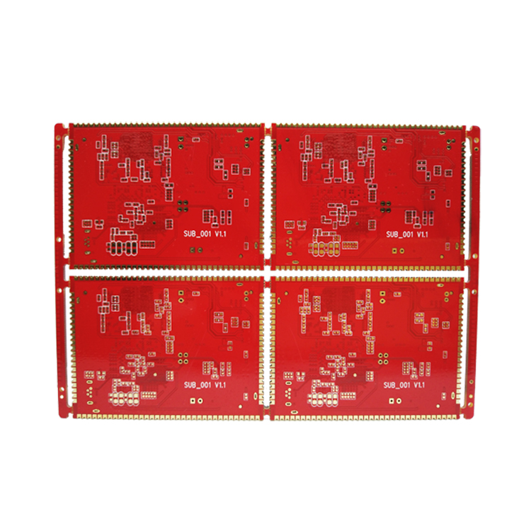
The PCB design is completed because the PCB shape is too small to meet the production process requirements, or a product is composed of several PCBs, so it is necessary to assemble several small boards into a large board with an area meeting the production requirements, or to assemble multiple PCBs for a product to facilitate the production of electrical equipment. The former is similar to the stamp board. It can not only meet the PCB production process conditions, but also facilitate the electrical installation of components. It is very convenient to separate them when using; The latter is to assemble several sets of PCB boards of a product together, which is convenient for production and is also convenient for a complete set of products.
Generation of optical drawing data
The base of PCB production is film base. In the early stage of making a film base, it is necessary to make a film base first, and then use the base to take photos or copy. The accuracy of the base drawing must be consistent with the requirements of the printed board, and compensation for the deviation caused by the production process should be considered. The base drawing can be provided by the customer or made by the manufacturer, but both parties should cooperate and negotiate closely to make it meet the user's requirements and adapt to the production conditions. If the user provides the base drawing, the manufacturer shall inspect and approve the base drawing, and the user can evaluate and approve the original version or the first printed board product.
The base map is made by hand drawing, mapping and CAD drawing. With the development of computer technology, the PCB CAD technology has made great progress, and the PCB production process level has also been rapidly improved to the direction of multi-layer, thin wire, small aperture, and high-density. The original film plate making process can no longer meet the design needs of PCB, so photo painting technology has emerged. The photo plotter can directly send the PCB graphic data file designed by CAD to the computer system of the photo plotter, and control the photo plotter to draw graphics directly on the negative film using light. Then, the film base is obtained by developing and fixing. The photo painting technology is used to make the printed circuit board film base plate, which is fast, accurate, and of good quality. It also avoids the human errors that may occur when manually mapping or drawing the base plate, greatly improves the work efficiency, and shortens the production cycle of the printed circuit board. Using our laser photo plotter, we can complete the work that many people used to do for a long time in a very short time, and the thin wires and high-density plates drawn by it are incomparable to manual operation.
According to the different structures of laser photo plotters, they can be divided into flat plate type, internal drum type and external drum type. The generation of photo drawing data is to convert the design data generated by CAD software into photo drawing data, modify and edit it through CAM system, and complete photo drawing preprocessing (plate assembly, mirror image, etc.) to meet the requirements of PCB production process. Then, the processed data is sent to the photo plotter, which is converted into raster data by the Raster image data processor of the photo plotter. The raster data is sent to the laser photo plotter through the high speed compression and restoration algorithm to complete the photo painting.
PCB manufacturing, PCB design and PCBA processing manufacturers will explain the details of the generation of pcb assembly light drawing data.


Just upload Gerber files, BOM files and design files, and the KINGFORD team will provide a complete quotation within 24h.