
Professional PCB manufacturing and assembly
Building 6, Zone 3, Yuekang Road,Bao'an District, Shenzhen, China
+86-13410863085Mon.-Sat.08:00-20:00

PCB proofing mounting hole and how PCB is manufactured
Pcb proofing installation hole
The mounting hole is the screw hole for fixing the board card. If it is not used for grounding, copper foil cannot be used within 5mm around. These holes are used for grounding, so there is a ring of copper foil around them. In this way, the ground wire of the board card is connected with the metal shell of the chassis through metal screws, which can play a shielding role
Datum point
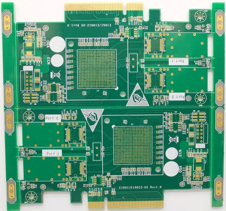
PCB proofing boards with a large number of SMD components usually have very dense components, and the pin arrangement of some large-scale integrated circuits is more dense. To use automatic equipment to place components on PCB, it requires very high precision To meet this requirement, a reference point is usually designed on the PCB to help the automation equipment align with the PCB A PCB usually has a global reference point and a local reference point. The two reference points seen on the diagonal of the entire PCB are global reference points, and the local reference points seen on the diagonal of components packaged with close spacing QFP, TSOP and BGA With these reference points, all components can accurately coincide with the positions designed on the PCB
How pcb proofing PCB is made
Take a motherboard at random. You may think it's incredible how such a complex circuit can be made into a PCB? To make a PCB, first use special software (such as Protel) to design the circuit schematic diagram, and then import the schematic diagram into the PCB design software for layout, that is, determine the position of each component on the PCB After the position is determined, the line drawing tool in the software is required to connect these components together. These lines are the actual copper foil on the PCB Wires cannot be crossed at will. Crossing means electrical connection. Only those allowed to be connected in the circuit schematic diagram can be crossed. Therefore, copper foil wires on our PCB are all zigzagged and twisted
After the PCB drawing is designed, it can be processed by the factory
It can be seen that the manufacturing of PCB is not so simple. If multilayer boards are manufactured, the processing technology is more complex and the cost is higher In fact, PCB accounts for a large proportion of the cost of computer boards, which is why some boards use the four layer board design to reduce the cost
In general, PCB design and manufacturing is a complex subject. Even the computer boards produced by small and inconspicuous factories on the market are designed by professional PCB engineers. When you buy computer boards, you might as well enjoy the beauty of PCB first


Just upload Gerber files, BOM files and design files, and the KINGFORD team will provide a complete quotation within 24h.