
Professional PCB manufacturing and assembly
Building 6, Zone 3, Yuekang Road,Bao'an District, Shenzhen, China
+86-13410863085Mon.-Sat.08:00-20:00

PCB manufacturer explains why PCB should be made into multi-layer
For the most basic PCB, the components are concentrated on one side and the wires are concentrated on the other side. Because only one side can be used for wiring, we call this PCB a single panel. Both sides of the double-sided board can be used for wiring, so the wiring area is twice that of the single panel, which is suitable for more complex circuits
For a simple circuit such as a radio, it is OK to use a single panel or a double-sided board to make it. However, with the development of microelectronics technology, the complexity of the circuit has greatly increased, which also puts forward higher requirements for the electrical performance of PCB. If a single panel or a double-sided board is also used, the circuit volume will be large, which also brings great difficulties to the wiring. In addition, electromagnetic interference between lines is not easy to deal with, Then there are multilayer boards (the number of layers represents several independent wiring layers, usually even)
The advantages of using multilayer plates are: high assembly density and small volume; The connection between electronic components is shortened, and the signal transmission speed is improved; Convenient wiring; For high frequency circuit, ground layer is added to make signal line form constant low impedance to ground; The shielding effect is good, but the more layers, the higher the cost, the longer the pcb proofing processing cycle, and the quality inspection is more troublesome
Our common computer boards usually use four or six layer boards, but now there are more than 100 layers of practical printed circuit boards. The difference between the six layer board and the four layer board is in the middle, that is, two internal signal layers are added between the ground wire layer and the power supply layer, which is thicker than the four layer board
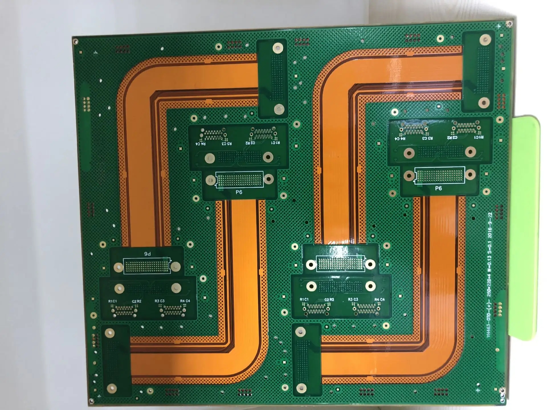
Multilayer boards are actually formed by laminating and bonding several etched single or double sided boards. Double sided boards are easy to distinguish. When looking at the light, except for the wiring on both sides, other places are transparent. For four layer boards and six layer boards, because the layers in the PCB are closely bonded, if there are corresponding marks on the board, there is no good way to distinguish them
Via (VIA) - the "bridge" of the circuit
After introducing multilayer boards, you may have a question in your mind that layers should be insulated. How do the circuits between them relate? In order to realize the electrical connection between layers, holes are punched on the insulation layer of PCB, and then copper is plated on the hole wall to connect the internal and external circuits. Such holes are called through holes, through holes or through holes. For multilayer boards, through holes are divided into several types: through holes that run through all layers, semi hidden holes that can only be seen on one side, and full hidden holes that cannot be seen
In addition to forming vias through electroplating, the method of filling the air with "conductive paste" to make conductive holes has also been popularized recently. Conductive paste is a paste of metal particles added into the resin. Once filled into the holes, once solidified, the metal particles can contact each other to connect the circuit. The holes thus formed are called metal conductive holes, and the holes formed by silver particle conductive paste are called "silver conductive vias". Recently, copper particle conductive paste has also been used
It can be seen that vias are the "bridge" to connect the circuit, but the "bridge" can not be built randomly. For the connection between two points, too many vias will lead to a decline in reliability
Knowledge of Wiring
Mistakes of serpentine line
In the trial reports of many boards, we can see a description like this: "The workmanship is good, and there are many snaking lines on the board". Maybe everyone's understanding of wiring starts from snaking lines, so what is the snaking line?
Generally speaking, the serpentine wire refers to the kind of wiring with continuous S-shaped changes. Intuitively, there is no obstacle between the two points to be connected, which could have been connected in a straight line, but the serpentine wire is actually used. Theoretically, the serpentine wire has these functions: forming a small inductance, restraining the change of signal current on the wire; Ensure the equal length of some lines; It can suppress crosstalk to a certain extent. It can be seen that this is only a local wiring method, and designers should use it according to the actual situation, not judging the quality of PCB wiring by the number of serpentine lines
Different in thickness
When we observe the PCB, we can find that the wiring is thick and thin. The thick part is usually the power line and ground wire, while the thin part is the data line. This is because the power line and ground wire should pass through a relatively large current, and should be as thick as possible. Therefore, the spare parts are often covered by pieces of copper foil as ground wires. The data line can be designed to be thin when the current passing through it is small, and the thin connection is more conducive to wiring
There are also some stresses on turning
The routing on the PCB cannot be all straight lines, so the problem of steering must be involved. The design usually requires that the routing should not be a right angle, but a 45 degree angle (referring to the clamping angle with the line extension direction). This is because the right angle and acute angle graphics will affect the electrical performance in high-frequency circuits, and it is easy to peel off under high temperatures. Therefore, it is usually required that the steering position of the routing should be an obtuse angle or a rounded corner
Colorful coat for pcb proofing PCB
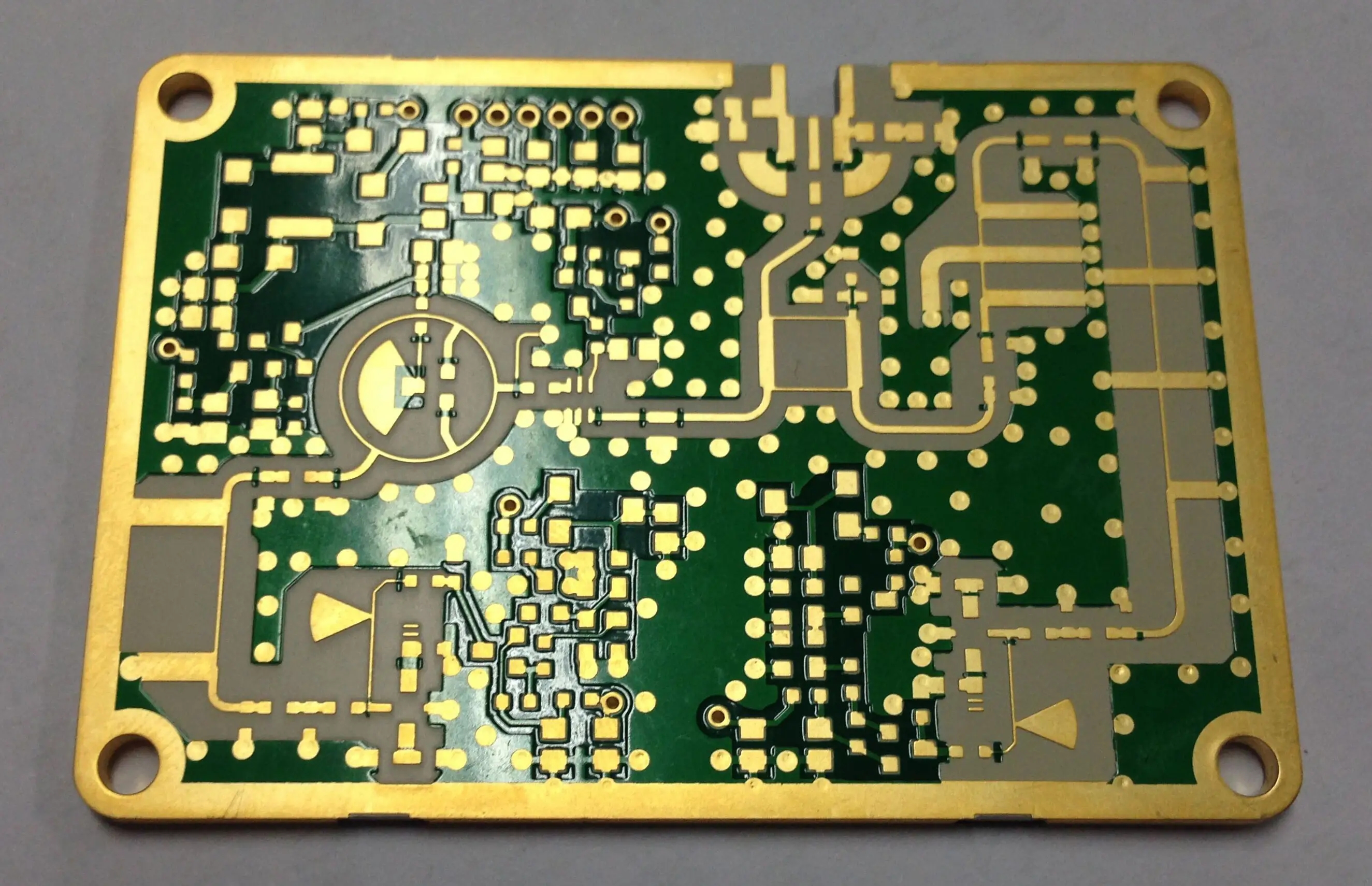
I'm afraid our first impression of the computer board is its color. In addition to the most common green and brown, there are blue, red, black, purple, and so on. What's the meaning of these colors? To answer this question, let's first think about why other copper wires on the PCB do not have tin. In addition to the bonding pads and other parts that need soldering, there is a layer of solder mask on the surface of the rest of the PCB, which is used to prevent bridge phenomenon during wave soldering, improve welding quality, save solder and other advantages. It is also a permanent protective layer of the PCB, which can prevent moisture and corrosion, Anti mildew, mechanical scratch and other functions. The solder mask is mostly green, so the solder mask oil is often called green oil in the PCB industry. The color of PCB is actually the color of solder mask oil. If the solder mask oil is added with other chemical materials, its color can be changed, but the color is only for decoration, and has no effect on the performance


Just upload Gerber files, BOM files and design files, and the KINGFORD team will provide a complete quotation within 24h.