
Professional PCB manufacturing and assembly
Building 6, Zone 3, Yuekang Road,Bao'an District, Shenzhen, China
+86-13410863085Mon.-Sat.08:00-20:00

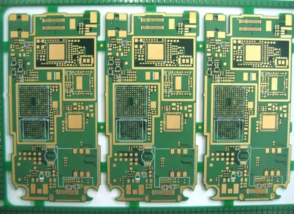
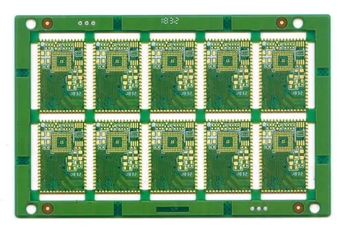
Methods and Steps of Copying PCB for PCB Proofing
The first step of pcb proofing is to get a PCB. First, record the models, parameters and positions of all the elements on the paper, especially the directions of diodes, three machine tubes and IC notches. It is better to take two photos of the position of the pneumatic parts with a digital camera.
In the second step of pcb proofing, remove all components and remove the tin from the PAD hole. Clean the PCB with alcohol, and then put it into the scanner. When the scanner scans, it needs to slightly raise some scanning pixels to get a clearer image. Start POHTOSHOP, scan the screen printing surface in color mode, save the file and print it for backup.
In the third step of pcb proofing, slightly polish the two layers of TOP LAYER and BOTTOM LAYER with water gauze until the copper film is bright, put them into the scanner, start PHOTOSHOP, and scan the two layers in color mode. Note that the PCB must be placed horizontally and vertically in the scanner, otherwise the scanned image cannot be used, and the file should be saved.
In the fourth step of pcb proofing, adjust the contrast and lightness of the canvas to make the part with copper film and the part without copper film have a strong contrast. Then turn the secondary image to black and white to check whether the lines are clear. If not, repeat this step. If the image is clear, save it as a black and white BMP file TOP.BMP and BOT.BMP. If you find a problem with the image, you can also use PHOTOSHOP to repair it.
In the fifth step of pcb proofing, convert two BMP files into PROTEL files, and transfer two layers into PROTEL. If the positions of PAD and VIA passing through the two layers basically coincide, the previous steps are well done. If there is any deviation, repeat the third step.
The sixth part of pcb proofing is to convert the BMP of the TOP layer to the TOP. PCB. Note that it should be converted to the SILK layer, which is the yellow layer. Then you can trace lines on the TOP layer and place devices according to the drawings in the second step. Delete SILK layer after drawing.
In the seventh step of pcb proofing, convert the BMP of the BOT layer to the BOT. PCB. Note that it should be converted to the SILK layer, which is the yellow layer. Then you can trace lines on the BOT layer. Delete SILK layer after drawing.
In the eighth step of pcb proofing, call TOP.PCB and BOT.PCB in PROTEL and combine them into one diagram.
In the ninth step of pcb proofing, use a laser printer to print the TOP LAYER and BOTTOM LAYER on the transparent film (1:1 ratio), place the film on that PCB, and compare whether there is any error. If it is correct, you will be finished.
Others: If it is a multilayer board, you should carefully polish it to the inner layer, and repeat the third to ninth steps. Of course, the naming of the figure is different. It should be determined according to the number of layers. Generally, the double-sided board is much simpler than the multilayer board. The multilayer board is prone to misaligned, so the multilayer board should be particularly careful and careful (the internal through hole and non through hole are prone to problems).
PCB manufacturing, PCB design, and PCBA processing manufacturers will explain the methods and steps of PCB copying for PCB proofing.


Just upload Gerber files, BOM files and design files, and the KINGFORD team will provide a complete quotation within 24h.