
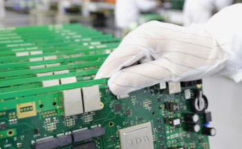
Professional PCB manufacturing and assembly
Building 6, Zone 3, Yuekang Road,Bao'an District, Shenzhen, China
+86-13410863085Mon.-Sat.08:00-20:00

Quality problems that may arise from substrate and laminate
It is impossible to manufacture any number of printed circuit boards without encountering some problems. Some of the quality reasons are attributed to the materials of copper clad laminate. When quality problems occur in the actual manufacturing process, it is often because the substrate material becomes the cause of the problem. Even a carefully written and practically implemented laminate technical specification does not specify the test items that must be carried out to determine that the laminate is the cause of the production process problems. Here are some of the most common laminate problems encountered and how to identify them. Once encountering laminate problems, it should be considered to add to the laminate material specification. Usually, if this kind of technical specification is not enriched, it will lead to continuous quality changes, and then lead to product scrapping. Generally, the material problems caused by the quality change of laminates occur in the products manufactured by manufacturers with different batches of raw materials or with different pressing loads. Few users can hold a large number of sufficient records to enable them to distinguish specific pressing loads or material batches at PCB processing sites. As a result, it often happens that the printed circuit board is continuously produced and installed with components, and continuous warping occurs in the solder slot, thus wasting a lot of labor and expensive components. If the loading batch number is immediately available, the laminate manufacturer can check the resin batch number, copper foil batch number, curing cycle, etc. That is, if the user cannot provide continuity with the laminate manufacturer's quality control system, the user will suffer long-term losses. The general problems related to substrate materials in the manufacturing process of printed circuit boards are described below.

1、 Superficial problems
Symptoms: poor adhesion of printing materials, poor adhesion of coating, some parts cannot be etched, and some parts cannot be soldered.
The inspection methods can be used: generally, water is used to form visible water lines on the board surface for visual inspection, or ultraviolet lamp is used to irradiate the copper foil to check whether there is resin on the copper foil.
Possible causes:
1. The very dense and smooth surface caused by the demoulding film makes the uncoated copper surface too bright.
2. Generally, the laminate manufacturer does not remove the mold release agent on the uncoated side of the laminate.
3. Pinholes on the copper foil cause resin to flow out and accumulate on the copper foil surface, which usually occurs on copper foil thinner than 3/4 oz weight specification, or environmental problems cause resin powder to be laminated on the copper foil surface.
4. Copper foil manufacturer applies excessive antioxidant on the surface of copper foil.
terms of settlement:
1. It is recommended that laminate manufacturers use fabric like films or other demoulding materials.
2. Contact the laminate manufacturer to use mechanical or chemical elimination methods.
3. Contact the laminate manufacturer to inspect each batch of copper foil that is unqualified; Ask for solutions to remove the resin and improve the manufacturing environment.
4. Ask the laminate manufacturer for removal method. It is generally recommended to use hydrochloric acid and then remove it mechanically.
5. Before any change in laminate manufacturing, cooperate with the laminate manufacturer and specify the user's test items.
2、 Appearance problems
Symptoms: obviously different colors of laminates, different surface colors, stains on the surface or inner layer, and thin layers of various colors on the surface of laminates
Inspection method: visual inspection.
Possible causes:
1. The glass cloth base plate has white cloth lines or white spots on the surface before processing or after etching.
2. After processing, there are more white spots or glass cloth exposed on the surface.
3. After processing, especially after soldering, there is a thin layer of white film on the surface, which indicates that it is slightly etched by resin or has foreign deposits.
4. The color change of the base material exceeds the possible acceptable appearance requirements
terms of settlement:
1. In rare cases, glass cloth is exposed due to lack of resin on the surface, which is rare today. It is more common to see tiny bubbles or small white holes on the surface. This is caused by the reaction between the glass cloth surface coating and the resin system. The surface resistivity of a board with a lot of glass cloth exposed decreases as the humidity increases. However, boards with tiny bubbles or small bubbles usually do not drop. Strictly speaking, this is just a problem of appearance. Contact the laminate manufacturer to avoid such a problem; And determine the internal standard of acceptable micro foaming.
2. Most of the glass cloth exposed after processing is due to solvent etching, which removes some surface resin. Check all solvents and plating solutions together with the laminate manufacturer, especially the time and temperature of the laminate in each solution to ensure that they are suitable for the laminate used. Where possible, process according to the conditions recommended by the laminate manufacturer.
3. Inspect with the laminate manufacturer to ensure that the flux used is suitable for the plate used. Verify the technological process that may deposit minerals or inorganic substances. In the technological process that may deposit minerals or inorganic substances, use water that has removed minerals as much as possible.
4. Contact the laminate manufacturer to ensure that any major components or resins of the laminate (which affect the color) are approved by the user before making changes. Sometimes excessive copper alloy transfer will affect the color. Work with the laminate manufacturer to determine the acceptable appearance range.
3、 Machining problems
Symptom: the processing quality of punching, shearing and drilling is inconsistent, the coating adhesion is poor or the coating is uneven in the metallized hole.
Inspection method: inspect the incoming materials, test various key machining operations, and conduct routine analysis after the incoming materials of the laminate are metallized through the hole.
Possible causes:
1. Material curing, resin content or plasticizer change will affect the drilling, punching and shearing quality of materials.
2. Poor drilling, punching or shearing process, resulting in poor or inconsistent production quality.
3. The preheating period before punching or drilling is too long, which sometimes affects the processing of laminates.
4. The aging of materials, mainly phenolic materials, sometimes leads to the loss of plasticizer in the materials, making the materials more brittle than usual.
terms of settlement:
1. Contact the laminate manufacturer to establish the test of key mechanical processing performance requirements for modeling. The production die shall not be used for test, otherwise the wear and change of the production die will affect the test results. In the case of any change in machinability, the quality of the laminate can only be suspected if the problem occurs at the same time as the change in the material batch number.
2. Refer to the manufacturing recommendations for various types of laminates. Contact the laminate manufacturer to find out the specific penetration rate, feed, bit and punch temperature for each grade of laminate. Keep in mind that each manufacturer uses different mixtures of resins and substrates, and their recommendations will be different.
3. Carefully preheat the laminate and be sure to find out any overheating areas, such as those under the heating lamp. When heating materials, the principle of first in first out shall be followed.
4. Inspect with the laminate manufacturer to obtain the aging characteristic data of materials. Turnover inventory, so that the inventory is usually newly produced plates. Be sure to find out possible overheating during storage in the warehouse.
4、 Warping and twisting problems
Symptom: the base material is warped or twisted before, after or during processing. Hole inclination after soldering is also a sign of base material warping and distortion.
Inspection method: float welding test may be used for incoming inspection. Soldering tests with a 45 degree tilt are particularly effective.
Possible causes:
1. The material warps or twists at the time of receipt or after sawing and shearing, which is usually caused by improper lamination, improper cutting or uneven laminate structure.
2. Warpage can also be caused by improper storage of materials, especially when the paper base platen is placed vertically, it will be arched or deformed
3. In the process of processing or soldering, the hole displacement or inclination on the material is caused by improper curing of the laminate or the stress of the base material glass cloth structure.
terms of settlement:
1. Straighten the material or release the stress in the oven, and cut off according to the tilt angle and plate heating temperature recommended by the laminate manufacturer. Contact the laminate manufacturer to ensure that the PCB substrate with unbalanced structure is not used.
2. Store the materials flat in the loading cardboard box or lay the materials flat on the shelf at an angle. Generally, the materials shall be placed at an angle of 60 degrees or less with the ground.
3. Contact the laminate manufacturer to avoid unequal copper foil on both sides. Analyze the plating and stress, or local stress caused by heavy components or large copper foil area. Redesign the printed circuit board to balance the area of components and copper. Sometimes, most of the wires on one side of the printed board are laid vertically with the wires on the other side, so that the thermal expansion on both sides is not equal, causing distortion. Whenever possible, such wiring should be avoided.
V White spots or layering of laminated plate
Symptoms: white spots or cloth patterns appear on the surface or in the material; It can occur locally or in large areas.
Inspection method: proper floating weld test.
Possible causes:
1. During soldering, large area of blistering is caused by moisture and volatile matter pressed into the material. Poor machining is also a reason, because it will delaminate the laminate and make it absorb water in the wet process.
2. White cloth lines or white spots are produced during tin welding, which is due to the uneven structure of the laminate, improper curing of the laminate, poor stress release of the laminate, or poor ductility of the plated copper.
3. Fiber or serious white spots are exposed during soldering operation. This is due to excessive contact with solvents, especially chlorine containing solvents, which can soften the resin.
4. When the base material is heated, the tightly fixed big bull or connecting terminal will cause great stress on the plate. The result is a white spot around this dense area. The plate is stressed immediately during or after immersion welding, and there will be white spots in bending or bending,
terms of settlement:
1. Notify the PCB laminate manufacturer and find out a batch of laminates with such problems. Use the recommended machining method for all PCB boards.
2. Contact the laminate manufacturer for instructions on how to release the stress on the printed board before immersion welding. The PCB will absorb excessive moisture after being stored for a period of time under high humidity, which will affect the solderability of the PCB. Pre drying and preheating the printed circuit board before the soldering operation to reduce thermal shock will help solve these two problems (refer to the moisture absorption data of the stored printed circuit board for multi-layer materials).
3. Contact the laminate manufacturer for the most appropriate solvent and length of application. When the substrate changes, verify all wet processing processes, especially solvents.
4. During wave soldering or manual soldering operation, loosen the fastened wiring terminals and remove any radiator or heavy components before immersion welding. Check the correctness of the machining operation, especially the punching operation, to ensure that the white spots are caused by slight delamination due to improper operation. Ensure that the plates are properly clamped with clamps and are not stressed when heated. Do not put the printed circuit board into the cold flux remover for quenching while it is hot or under stress.
VI Bond strength problem
Symptom: During the immersion welding process, the bonding pad and the wire are separated.
Inspection method: fully test and carefully control all wet processing processes during incoming inspection.
Possible causes:
1. During PCB processing, pad or wire separation may be caused by electroplating solution, solvent etching or copper stress during electroplating operation.
2. Punching, drilling or perforating will make the pad partially detached, which will become obvious during hole metallization operation.
3. In the process of wave soldering or manual soldering, the bonding pad or wire separation is usually caused by improper soldering technology or excessive temperature. Sometimes the bonding pad or wire is detached because the laminate is not well bonded or the thermal peeling strength is not high.
4. During soldering operation, the absorbed heat retained by PCB components will cause the pad to detach.
terms of settlement:
1. Give the laminate manufacturer a complete list of solvents and solutions used, including the processing time and temperature of each step. Analyze whether copper stress and excessive thermal shock occur in electroplating process.
2. Follow the mechanical processing method of pushing. The problem can be controlled by frequent analysis of metallized holes.
3. Most PCB pads or wires are detached due to lax requirements for all operators. If the temperature inspection of the solder pot fails or the dwell time in the solder pot is prolonged, the solder pot will also disengage. In the manual tinning repair operation, the pad separation is probably caused by the use of electric ferrochrome with improper wattage and the failure to carry out professional process training. Now some laminate manufacturers, for strict tin welding use, have manufactured laminates with high peel strength at high temperatures.
5. If possible, remove the heavy components from the whole printed board, or install them after immersion welding. Usually, a low wattage electric soldering iron is used for careful soldering. Compared with component immersion soldering, the substrate material is heated for a shorter duration.
7、 Excessive size change
Symptom: after processing or soldering, the size of the base material exceeds the tolerance or cannot be aligned.
Inspection method: fully control the quality during processing.
Possible causes:
1. The texture direction of paper-based materials is not paid attention to, and the forward expansion is about half of the horizontal expansion. Moreover, the substrate cannot be restored to its original size after cooling.
2. If the local stress in the laminate is not released, it will sometimes cause irregular size changes during processing.
terms of settlement:
1. Instruct all production personnel to cut the plates in the same texture direction. If the size change exceeds the allowable range, the base material can be used instead.
2. Contact the PCB laminate manufacturer for advice on how to release material stress before PCB manufacturing.


Just upload Gerber files, BOM files and design files, and the KINGFORD team will provide a complete quotation within 24h.