
Professional PCB manufacturing and assembly
Building 6, Zone 3, Yuekang Road,Bao'an District, Shenzhen, China
+86-13410863085Mon.-Sat.08:00-20:00

In high-speed PCB design, the continuity of controllable impedance plate and line impedance is a very important problem. The common impedance is 50 Ω at single end and 100 Ω at difference. How to ensure the signal integrity? In our common way, the adjacent layers of signal lines have complete GND planes, or power planes. We use SCM to make products. Generally, we do not need to do impedance, and its working frequency is generally very low. You can learn the method of impedance calculation by clicking SI9000. Next, we will learn the basic knowledge of PCB design together with Shenya Electronics.

Set up techniques
Different settings are required in different stages of the design, and large grids can be used for device layout in the layout stage; For large devices such as IC and non positioning connector, the grid point accuracy of 50-100 mil can be selected for layout, while for passive small devices such as resistance, capacitance and inductance, the grid point of 25 mil can be used for layout. The accuracy of large grid points is conducive to the alignment and beautiful layout of devices. In high-speed cabling, we generally use millimeter mm as the unit, and we mostly use mil as the unit.
PCB layout rules
1. In general, all components should be arranged on the same side of the circuit board as much as possible. Only when the top layer components are too dense can some devices with limited height and low heat generation, such as patch resistance, patch capacitance, and patch chip, be placed on the bottom layer.
2. On the premise of ensuring the electrical performance, the components shall be placed on the grid and arranged in parallel or vertical to each other, so as to be neat and beautiful; The elements shall be arranged compactly, and the elements shall be evenly distributed and uniformly spaced throughout the layout.
3. The distance between the device and the edge of the circuit board is generally not less than 2MM, and the process is 5mm. When the distance is less than 5MM, we should process the edge. Of course, the mechanical strength that the circuit board can withstand should also be considered.
Layout Skills
In the layout design of PCB, the unit of the circuit board shall be analyzed, and the layout design shall be carried out according to the function. The layout of all components of the circuit shall comply with the following principles:
1. Arrange the position of each functional circuit unit according to the circuit flow, so that the layout is convenient for signal flow and the signal is kept in the same direction as far as possible.
2. Centered on the core components of each functional unit, the layout is carried out around it. The components and parts shall be evenly, integrally and compactly arranged on the PCB to minimize and shorten the leads and connections between components and parts. When the interface is fixed, we should arrange the interface, then the core components. The shortest high-speed signal is the principle.
3. For circuits operating at high frequencies, the distribution parameters between components should be considered. Low frequency and high frequency line circuits shall be separated, and digital and analog circuits shall be designed separately.
Layout design
In PCB, special components refer to the key components in the high-frequency part, the core components in the circuit, the components susceptible to interference, the components with high voltage, the components with high heat, and some heterosexual components. The positions of these special components need to be carefully analyzed, and the tape layout should meet the requirements of circuit functions and production requirements. Improper placement of them may cause circuit compatibility problems and signal integrity problems, which may lead to PCB design failure.
Placement order
1. Place components closely matching with the structure, such as power socket, indicator light, switch, connector, etc.
2. Place special components, such as large components, heavy components, heating components, transformers, ICs, etc.
3. Place small components.
Layout check
1. Whether the size of circuit board is consistent with the processing size required by CAD drawings.
2. Whether the layout of components is balanced, orderly arranged and completely distributed.
3. Whether there are conflicts at all levels. Whether the components, frames and connectors are reasonable.
4. Whether the commonly used components are convenient for maintenance and installation. Such as switches, plug-in devices, components that must be replaced frequently, etc.
5. Whether the distance between thermal components and heating components is reasonable.
6. Whether the heat dissipation is good.
7. Whether the interference of the line needs to be considered.
Wiring principle
1. Avoid arranging important signal lines at the edge of PCB, such as clock and reset signal.
2. The space between the casing ground wire and the signal wire shall be at least 2mm
3. The high-speed signal shall be drilled as small as possible to ensure the integrity of the signal.
4. Whether the digital and analog signals are separated. Whether high frequency and low frequency signals are separated.
5. In the design of large area copper coating, there shall be a window on the copper coating, with heat dissipation holes, and the window shall be designed as a mesh.
6. Whether the vibrating crystal and transformer are wired below. Only if we practice hard can we improve our basic knowledge day by day.
Silk screen placement
1. The silk screen tag number is not welded, and it is missing after the silk screen is placed for production.
2. The silk screen tag number is clear, and the recommended word width/height is 4/25mil, 5/30mil, and 6/45mil.
3. Keep the direction uniformity. Generally, one PCB should not be placed in more than two directions. It is recommended to place the letters on the left or below
Network DRC check and structure check
Quality control is an important part of PCB design process. General quality control means include: design self inspection, design mutual inspection, expert review meeting, special inspection, etc.
Schematic diagram and structure element diagram are the most basic design requirements. Network DRC inspection and structure inspection are to confirm that PCB design meets the two input conditions of schematic network table and structure element diagram respectively.
Regular assembly
In the design, from the perspective of PCB assembly, the following parameters should be considered:
1. The diameter of the hole shall be determined according to the maximum material condition (MMC) and minimum material condition (LMC). The diameter of a hole without supporting components should be selected in such a way that the MMC of the pin is subtracted from the MMC of the hole, and the difference is between 0.15 and 0.5 mm. Moreover, for ribbon pins, the difference between the nominal diagonal of the pin and the inner diameter of the unsupported hole will not exceed 0.5mm and not less than 0.15mm.
2. Place smaller components reasonably so that they will not be covered by larger components.
3. The thickness of resistance welding shall not be greater than 0.05mm.
4. The screen printed identification shall not intersect with any pad.
5. The upper half of the circuit board should be the same as the lower half to achieve structural symmetry. Because asymmetrical circuit boards may become bent.
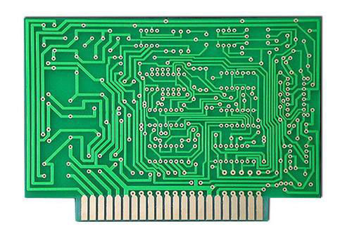
You can download a PCB online for comparison according to the above basic knowledge. We can also find and optimize a ready-made board.

How fast and good is PCB component layout?
Nov 05,2022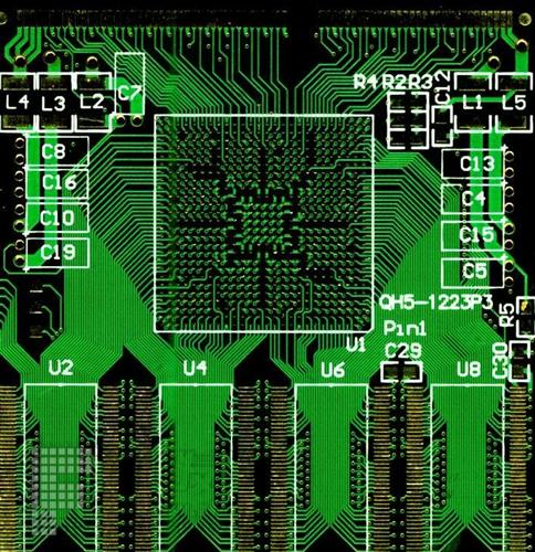


Just upload Gerber files, BOM files and design files, and the KINGFORD team will provide a complete quotation within 24h.