
Professional PCB manufacturing and assembly
Building 6, Zone 3, Yuekang Road,Bao'an District, Shenzhen, China
+86-13410863085Mon.-Sat.08:00-20:00

PCB screen printing specifications There are many specifications for PCB screen printing technology, which can not be done casually. These specifications promote the development of PCB screen printing technology. Let's take a look at the specifications: all components, mounting holes, and positioning holes have corresponding specifications
PCB silk screen specification
PCB screen printing technology has many specifications, which can not be done casually. These specifications have promoted the development of PCB screen printing technology. Let's take a look at the specifications:
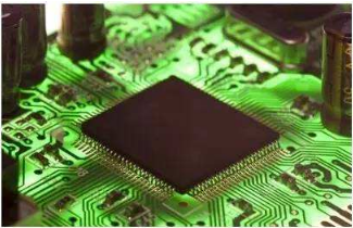
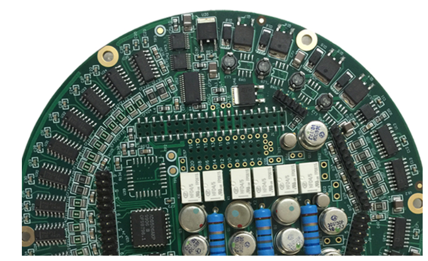
All PCB components, mounting holes and positioning holes have corresponding silk screen labels to facilitate the installation of finished boards. All components, mounting holes and positioning holes have corresponding silk screen labels. The silk screen of mounting holes on PCB is identified by H1, H2... Hn.
Silk screen characters shall follow the principle of from left to right and from bottom to top. Silk screen characters shall follow the principle of from left to right and from bottom to top as far as possible. For polar devices such as electrolytic capacitors and diodes, the direction shall be consistent in each functional unit as far as possible.
There is no silk screen on the device bonding pad and tin path that needs tin coating, and the device tag number should not be covered by the device after installation. (except for PCB with high density that does not need silk screen)
In order to ensure the PCB welding reliability of devices, it is required that there is no silk screen on the device pad; In order to ensure the continuity of tin coating, it is required that there is no silk screen on the tin coating; In order to facilitate device insertion and maintenance, the device tag number shall not be covered by the device after installation; The silk screen shall not be pressed on the through hole and pad to avoid the loss of part of the silk screen when the resistance welding window is opened, which will affect the identification. The screen spacing is greater than 5mil.
The polarity of polar components is clearly shown on the silk screen diagram, and the polarity direction marks are easy to identify.
The number of PCB photo files is correct, each layer should have correct output, and a complete number of layers should be output.
The identifier of PCB components must be consistent with the identification symbol in the BOM list.
The direction of the directional connector is clearly indicated on the silk screen.
The PCB shall be provided with barcode position identification. If the space on the PCB surface allows, the PCB shall be provided with 42 * 6 barcode silk screen frame. The position of the barcode shall be convenient for scanning.
The silk screen position of PCB name, date, version number and other information of the finished board shall be clear. PCB documents shall be printed with board name, date, version number and other board information, with clear and striking location.
PCB must have complete relevant information and anti-static identification of PCB manufacturer.
Key indicators of PCBA processing plant
Oct 25,2022


Just upload Gerber files, BOM files and design files, and the KINGFORD team will provide a complete quotation within 24h.