
Professional PCB manufacturing and assembly
Building 6, Zone 3, Yuekang Road,Bao'an District, Shenzhen, China
+86-13410863085Mon.-Sat.08:00-20:00

Best practice on how to avoid PCB failure
In this era of best technological innovation, all manufacturing organizations, original equipment manufacturers, small and medium-sized enterprises, electronic equipment and instruments have fully penetrated into large companies and enterprises Even an hour of downtime or electronic failure will cause considerable losses In addition, one of the root components of any equipment or machine is a printed circuit board, whether it is a simple or complex PCB layout or PCB components When the PCB is placed in the external environment, the possibility of failure will increase due to pollution, humidity or any type of thermal conditions Due to the need for PCB repair, PCB rework, machine/equipment depreciation, low asset life expectancy, indirect impact on work efficiency, fast turnover, order delivery delay, and high defects, financial impact may be caused Mass production and more production problems There are some simple remedial measures that people can practice on their own to strengthen PCB as an advanced defensive measure against failures in the external environment Read more about which solution is best for your PCB distribution
What is the best practice to avoid PCB failures
One of the common causes of circuit board failure in the external environment is mainly due to the moisture/humidity on the circuit board. When deploying printed circuit boards, there are now different types of solutions to protect them from moisture. Whether it is outdoor sensor system, high-energy motor controller, high-power battery charger, industrial load tester, ultrasonic technology, water treatment plant, robot cable components, aerospace, electronic equipment, marine technology, extreme outdoor PCB applications in telecommunications projects when PCB components or military use, and when PCB is exposed to humid environment, Defensive equipment, condensation, and other uncertainties caused by hazardous weather reactions may damage the circuit.
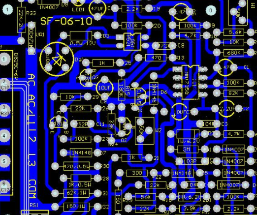
Circuit board

In addition to chemical, industrial, medical, robot, metal processing foundry, automobile industry, glass factory, microprocessor industry, agricultural sector, aviation operations, electronic banking and telecommunications industries, all face such problems. Renewable energy, seawater treatment and the whole power plant.
The simplest measure to prevent PCB failure due to moisture intrusion in the external environment:
PCB shall be equipped with tight housing and firm sealing system In some cases, a sturdy custom housing is required to protect the PCB from moisture This includes the situation that housing needs to be opened regularly; Drill holes in the housing due to circuit wiring or other environmental conditions Place the PCB in the box or box The housing shall have round sides to allow rapid drainage of condensate from the PCB In addition, you can also use desiccants to absorb the moisture in the box Apply a suitable conformal coating to the printed circuit board When selecting coating materials, the characteristics to be concerned include moisture resistance, chemical resistance or temperature range coating, high moisture resistance, air gap on the circuit board, rain, corrosive chemicals, salt water, pesticides, rapid thermal change or any other uncertain external climate It is recommended to consult professional PCB manufacturers to understand the required flow rate and viscosity of PCB conformal coating, which proves that there are many solder joints. When the circuit board has high flexibility, sharp edges and irregular terrain on the printed circuit board Protective materials such as silicone or epoxy resin are embedded into the entire PCB to pre protect the PCB from external objects PCB manufacturing This technology now has many options to achieve low thermal expansion and high thermal conductivity to eliminate problems related to temperature control and solder joint strain Using effective PCB layout software can help to incorporate component specifications for embedded design In addition, it helps to verify and track the appropriate composition of specific information or coatings
PCB failure caused by thermal conditions in outdoor environment:
In many cases, outdoor electrical equipment or equipment located in the control cabinet eventually fails or shuts down due to thermal conditions. Too low or too high temperature will cause great fluctuations, leading to PCB rework or repair. When installed in the external environment, overheating of electrical equipment or prolonging the service life of internal electronic equipment is a hot issue of concern. On the other hand, harsh or difficult hot weather includes the presence of solvents, oils, corrosive substances, sugar, corrosive substances, salt water, fibers or the risk of dusty environment. This can be done simply to avoid PCB failure during thermal problems. These include:
Regularly calculate the internal heat of the circuit board to be balanced Try to select the correct IP according to the type of harsh environment Make efforts to determine better heat dissipation solutions and appropriate installation process types according to the installation purpose and the climate response type of the installation location It is necessary to regularly track and measure humidity (dry, humid or very humid) and air temperature (maximum average temperature) Strict inspection of the installation area will help to obtain the actual restraint to which electrical equipment will be exposed Regularly analyze and measure the air quality at the installation site

Explain the process of PCB plug hole
Oct 23,2022


Just upload Gerber files, BOM files and design files, and the KINGFORD team will provide a complete quotation within 24h.