
Professional PCB manufacturing and assembly
Building 6, Zone 3, Yuekang Road,Bao'an District, Shenzhen, China
+86-13410863085Mon.-Sat.08:00-20:00

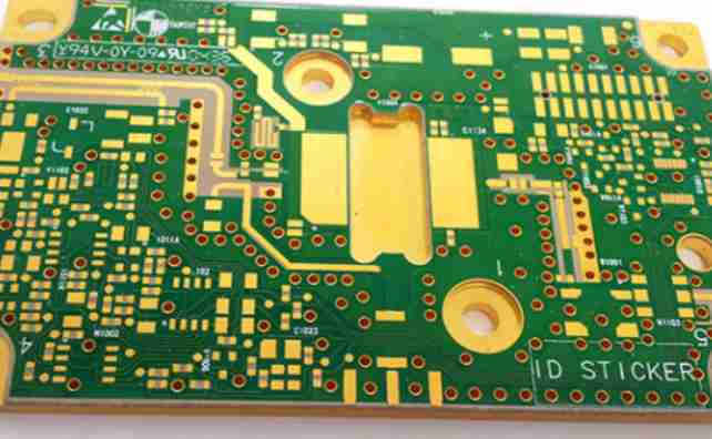
1, in the substrate, the welding pad of the DIE must be in the direction of the binding line, and the leading line also needs to be in the direction of the welding pad. For each DIE, a cross-shaped welding pad must be placed in its diagonal position as the alignment coordinate of the binding. The coordinate needs to be connected to the network of the attachment, which is generally selected (there must be a network, otherwise the cross will not appear). In order to prevent the cross from being submerged in copper and unable to be accurately positioned, it is generally surrounded by a frame that prohibits laying copper plates.
The bonding of DIE should be noted that unused pads, i.e. pads without network connection, need to be removed. As shown in the following picture.
2. The production process of the substrate is special, and each line must be cast by the electroplating line using the electroplating method to form the copper and the welding pad and the wire, or all other places where copper is needed. It must be noted here that even if the pad has no electrical connection or no network, it must be copper plated by pulling the pad out of the frame in eco mode, otherwise the pad will be copper-free. And the electroplating line that pulls out the plate frame must have a copper skin in other layers to mark its corrosion position, here with the seventh layer of copper skin to mark. In general, the copper is 0.15mm beyond the frame, and the copper-covered edge is about 0.2mm away from the frame.
3, in the board frame, to determine the positive and negative, it is best to place all devices on the same side, which is marked with three XXX, as shown in the figure below.
4. The pad used for the substrate is larger than the general pad and has a special package, which is CX0201, the difference between X mark and C0201. The arrangement is as follows:
0603 pad: 1.02mmX0.92mm pad window area: 0.9mmX0.8mm, the middle distance between the two pads is 1.5mm.
0402 pad: 0.62mmX0.62mm pad window area: 0.5mmX0.5mm, the middle distance between the two pads is 1.0mm.
0201 pad: 0.42mmX0.42mm pad window area: 0.3mmX0.3mm, the middle distance between the two pads is 0.55mm.

5, DIE requirements are as follows: binding pad (single wire) minimum size 0.2mmX0.09mm90 degrees, the spacing of each pad minimum 2MILS, the inner row of ground and power line pad width is also required to be 0.2mm. The Angle of the bonding pad should be adjusted according to the Angle of the component wire. The Substrate binding wire is not easy to be too long. The minimum distance between the main control DIE and the inner bonding pad is 0.4mm, and the minimum distance between the FLASHDIE and the bonding pad is 0.2mm. The length of the cable should not exceed 3mm. The spacing between the two rows of bonding pads should be more than 0.27mm apart.
6, the SMT pad and DIE binding pad and SMT components should be maintained at more than 0.3mm, and the distance between the binding pad of a DIE and another DIE should also be maintained at more than 0.2mm. The minimum signal route is 2MILS and the interval is 2MILS. The main power line is best to be 6-8MILS, and the floor is paved as large as possible. Where the floor cannot be paved, power and other signal lines can be laid to enhance the strength of the substrate.
7, wiring should pay attention to the hole and the pad, the line, the gold finger can not be too close, the same property of the master and the finger should be kept at least 0.12mm above, different properties of the hole as far as possible away from the pad and the finger. The minimum hole should be 0.35mm outside the hole and 0.2mm inside the hole. When laying copper, it should also be noted that the copper and the gold finger can not be very close to each other, some broken copper should be deleted, and a large area is not allowed to exist where the copper is spread.
8. When laying COPPER, use a grid, the ratio is 1:4, that is, COPPERPOUR is 0.1mm and copper is 0.4mm. The copper coating Angle is 45 degrees.
SMT processing soldering tip maintenance and use methods
The quality of SMT welding is related to the performance, reliability and production cost of electronic products. Therefore, how to make SMT machining and welding to achieve high quality and low consumption has always been the concern and research topic of the electronics industry. SMT welding quality management should be a systematic project. According to its content, it should generally include all personnel quality training, pre-welding quality inspection, welding quality prosecution, post-welding quality inspection and storage management.
1, the preparation before the use of welding table
First check and clean whether the sponge is soaked with water, first clean the sponge wet water, and then squeeze the remaining water. Only in this way can the lead-free soldering iron head get outstanding cleaning effect. If a non-moist cleaning sponge is used, the nozzle will be damaged and will not be tinned.
2, SMT processing and welding operation maintenance
Before welding, clean the impurities on the nozzle with a cleaning sponge, which can ensure that the quality of the solder joint will not show virtual welding, false welding, and can slow down the oxidation rate of the nozzle. Therefore, ensure that the cleaning degree of the nozzle can extend the service life of the nozzle.
3. Maintenance of welding table after welding operation
First set the temperature to 300 ° C, and then clean the nozzle, plus a layer of new solder for maintenance, so that the nozzle and air barrier can be maintained, the nozzle will not react with oxygen in the air.
4. Maintenance when the welding table is not used
When the welding table is not used, the nozzle should not be in a high temperature condition for a long time, which will convert the flux on the soldering iron head into oxide, resulting in a great decline in the thermal conductivity of the soldering iron head. When the welding table is not in use, the power should be turned off (for non-temperature control and no active sleep function of the welding table).
Five key points of PCB board design
Jun 19,2023


Just upload Gerber files, BOM files and design files, and the KINGFORD team will provide a complete quotation within 24h.