
Professional PCB manufacturing and assembly
Building 6, Zone 3, Yuekang Road,Bao'an District, Shenzhen, China
+86-13410863085Mon.-Sat.08:00-20:00

I. Purpose:
Standardize the process design of printed led circuit boards, meet the requirements of the manufacturability design of printed circuit boards, provide printed circuit board process design criteria for hardware designers, and provide process audit criteria for the manufacturability of printed circuit boards.
Ii. Scope:
This specification specifies the process design requirements that hardware designers should follow when designing printed circuit boards, and is applicable to all printed circuit boards designed by the company.
3. Special definition:
printed circuit board (PCB) :
A printed board forming a printed element or a printed circuit or a combination of both conductive patterns according to a predetermined design on an insulating substrate.

Component Side:
The main device (IC and other main devices) and the printed circuit board side of most components are installed, which is characterized by complex devices and has a greater impact on the printed circuit board assembly process. It is usually defined as the Top surface.
Solder Side: Solder side:
The other side corresponding to the component surface of the printed circuit board is characterized by relatively simple components. It is usually defined in terms of Bottom.
Plated Through Hole:
A hole in which metal is deposited on the wall. It is mainly used for electrical connection of conductive patterns between layers.
Nonmetallic hole (Unsupported hole) :
Holes not coated with electroplating or other conductive material.
Lead hole (component hole) :
A metallization hole on a printed circuit board used to electrically connect component leads to a printed circuit board conductor.
Through Hole:
Short for metallized Hole Through Connection.
Blind via:
Metallization hole for conducting pattern electrical connection between outer layer and inner layer of multi-layer printed led circuit board.
Buried Via:
Metallized holes for conducting pattern electrical connections between layers of multi-layer printed led circuit board.
Test hole:
Electrical connection holes designed for testing the electrical performance of printed circuit boards and printed circuit board components.
Mounting hole:
For the mechanical fixing foot of the component, the hole of the fixed component on the printed circuit board can be a metallized hole or a nonmetallic hole, and the shape depends on the need.
Plug hole:
Block the through hole with solder resistance ink.
Solder Mask, Solder Resist: Solder mask, solder resist:
A coating used to provide dielectric and mechanical shielding during and after welding.
Pad (Land, Pad) :
Conductive graphics for electrical connection and component fixation or both.
For other printed circuit terms and definitions, see GB2036-80 Printed Circuit Terms and Definitions.
Component Lead: A single or multiple strand of metal wire extending from a component as a mechanical or electrical connection, or a wire that has been formed.
Clinched Lead: The component lead is passed through the mounting hole of the printed board before welding and the formed lead is bent.
Axial Lead: The lead that extends along the axis of the component.
Wave Soldering (Wave Soldering) : The welding process in which a printed board is in contact with a continuously circulating wave shaped flow solder.
Reflow Soldering (Reflow Soldering) : It is a welding method that the welding end face of the components and the PCB welding pad are coated with paste solder and assembled together, heated until the solder is melted, and then the welding area is cooled.
Solder Bridging: Excess conductive path between wires formed by solder.
Solder Ball: A small ball of solder that forms on the surface of the laminate, solder shield, or wire (usually after wave soldering or reflow soldering).
Solder Projection: Excess solder bulges that appear on solidified solder joints or coats.
Tombstone Component: A defect in a double-ended chip element with only one metallized end welded to the pad and the other metallized end tilted away from the pad.
Integrated Circuit Package abbreviation:
Ball Grid Array (BGA) : Ball grid array, a type of surface array package.
QFP (Quad Flat Package) : square flat package.
PLCC (Plastic Leaded Chip Carrier) : plastic leaded chip carrier.
DIP (Dual In-line Package) : dual in-line package.
SIP (Single inline Package) : indicates a single-inline package
SOP (Small out-of-line Package) : small form factor package.
SOJ (Small out-of-line J-Leaded Package) : J-lead small shape package.
COB (Chip on Board) : chip on board package.
Flip-Chip: inverted welding chip.
CHIP components (CHIP) : Chip components are mainly passive components such as chip resistors, chip capacitors, and chip inductors. According to the different pins, there are full-terminal components (that is, the component lead terminal covers the entire end of the component) and non-full-terminal components, general ordinary chip resistors and capacitors are full-terminal components, and such as tantalum capacitors are non-full-terminal components.
THT (Through Hole Technology) : Through hole insertion technology
Surface Mount Technology (SMT) : surface mount technology
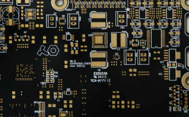
Component layout
General rules for component layout
Under the conditions of the design permit, the layout of the components should be arranged in the same direction as far as possible, and the modules with the same function should be arranged together; Components in the same package are placed equidistant for component mounting, welding and inspection.
PCB base board design principles
Jun 17,2023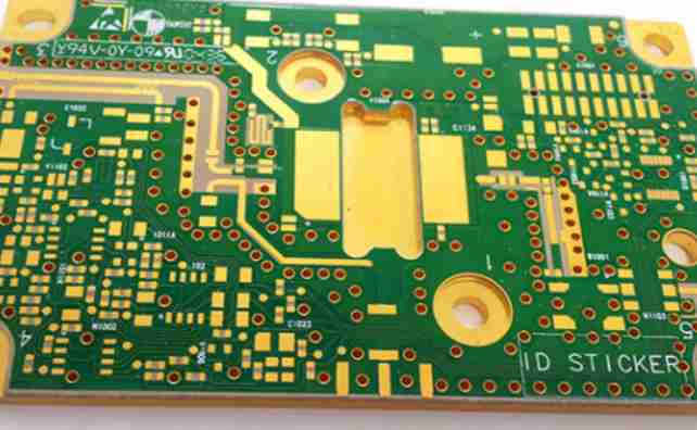


Just upload Gerber files, BOM files and design files, and the KINGFORD team will provide a complete quotation within 24h.