
Professional PCB manufacturing and assembly
Building 6, Zone 3, Yuekang Road,Bao'an District, Shenzhen, China
+86-13410863085Mon.-Sat.08:00-20:00

The distance between the legs of the standard components is 0.1 inches (2.54mm), so the basis of the grid system is generally set at 0.1 inches (2.54mm) or an integral multiple of less than 0.1 inches, such as: 0.05 inches, 0.025 inches, 0.02 inches, etc.
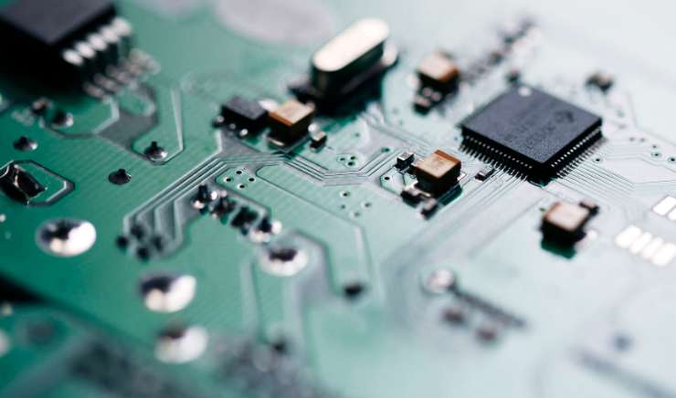
Design Rule Checking (DRC)
After the wiring design is completed, it is necessary to carefully check whether the wiring design meets the rules formulated by the designer, and it is also necessary to confirm whether the rules formulated meet the needs of the printed board production process, the general inspection has the following aspects:
Whether the distance between wire and wire, wire and component pad, wire and through hole, component pad and through hole, through hole and through hole is reasonable, whether it meets the production requirements.
Is the width of the power line and ground line appropriate, and is there a tight coupling between the power supply and ground line (low wave impedance)? Is there any place in the PCB that can make the ground wire wider?
Whether the best measures are taken for the key signal lines, such as the shortest length, the protection line, the input line and the output line are clearly separated.
Whether the analog circuit and the digital circuit have their own ground lines.
Whether the graphics (such as ICONS, marking) added to the PCB will cause signal short circuit.
Modify some undesirable lines.
Is there a process line on the PCB? Whether the solder resistance meets the requirements of the production process, whether the solder resistance size is appropriate, whether the character mark is pressed on the device pad, so as not to affect the quality of Denso.
Whether the edge of the outer frame of the power supply layer in the multi-layer board is reduced, such as the copper foil of the power supply layer is exposed outside the board, which is easy to cause short circuit.

The mobile power supply plays a role of small body and large function, which needs to be regulated by a special circuit through voltage conversion to achieve charging support for special products. This is just a small principle of the mobile power circuit board, the following by the mobile power wholesale manufacturers to explain the mobile power circuit board principle in detail. Let's have a look!
Compared with the huge battery, the circuit board can only be regarded as a "small body" accessory in the components of the mobile power supply, but you must not underestimate it. It is as if the same engine is matched by Mercedes and Chery models, but the actual driving performance is definitely better than Mercedes, which is the credit of the control system responsible for power distribution and conversion inside the car, and the circuit board of the mobile power supply is playing this role.
In simple terms, whether it is an 18650 cell or a lithium polymer battery, there is a safe charging cutoff voltage and a safe discharge cutoff voltage, as well as a rated maximum operating current. The basic function of the circuit board is to provide a safe and reliable charge management system for the battery. When charging the phone (when the battery is discharged), the battery is raised to a 5V booster system. At present, most of the circuit boards of mobile power supplies on the market are composed of the input charge control circuit, the output DC/DC conversion circuit, the battery power detection and display circuit, the charging indicator circuit, and the battery protection and intelligent management circuit.
PCB manufacturers talk about board requirements
First, circuit board plate
According to the grade level from bottom to high divided as follows:
94HB/94VO/22F/CEM-1/CEM-3/FR-4
The details are as follows:
94HB: ordinary cardboard, not fireproof (lowest grade material, die punching, can not be used as a power board)
94V0: Flame retardant board (die punching)
22F: Single side half glass fiber board (die punching)
Cim-1: Single glass fiber board (must be computer drilling, can not die punching)
Cim-3: double-sided half-glass fiber board (in addition to double-sided cardboard is the lowest end of the double-panel material, simple double-panel can be used with this material, than FR-4 will be cheaper 5~10 yuan/square meter)
FR-4: double-sided fiberglass board
Two, circuit board copper foil thickness
0.5 oz (18um), 1 oz (35um), 2 oz (70um).
Three, plate/plate requirements
1, plate thickness: 1.6mm
2, Material: FR4(International) 94V-0 with CE TUV ROHS certification
3, copper thickness: 1 ounce (35um) or more
4, process: spray tin, mechanical holes need 2 times drilling size accurate screen printing clear through the hole covered with green oil
5, the number of layers: double-sided
6. Metallization aperture tolerance: ±0.05mm
7, hole tolerance: ±0.05mm
8. Color: Green film
9. The characters on the pad do not need to be done, and the characters not on the pad are required to be done.
10. When the screen printing line passes through the character or pad, the screen printing line is disconnected.
11. In the slot opened on the pad, the part of the hole on the pad is made of metal holes, and the part of the pad is not made of non-metal holes.
12. The slot opened on the PCB is made into a non-metallic hole on the non-pad.
13. If the copper foil part is too close to the edge of the plate, or beyond the edge of the plate, cut the edge directly.
14, artboard software AD10 or Protel99SE
Four, steel mesh
General requirements: 47*37
Automatic solder paste requirements: 42*52 steel mesh, can be placed the size of the circuit board 300 (long) *250 (wide).

Problems encountered in PCB circuit board design
Jun 15,2023


Just upload Gerber files, BOM files and design files, and the KINGFORD team will provide a complete quotation within 24h.