1、 PCB component layout inspection rules
During

, after the system layout is completed, the PCB drawing shall be reviewed to see whether the system layout is reasonable and can achieve the optimal effect. Generally, the following aspects can be considered:
1. Whether the system layout can ensure the reasonable or optimal wiring, whether it can ensure the reliable wiring, and whether it can ensure the reliability of circuit work. In the layout, it is necessary to have an overall understanding and planning of the signal direction and the power and ground network.
2. Whether the size of the printed board is consistent with the size of the processing drawing, whether it meets the requirements of PCB manufacturing process, and whether it has behavior marks. This requires special attention. The circuit layout and wiring of many PCB boards are designed beautifully and reasonably, but the precise positioning of the positioning connector is neglected, which makes the designed circuit unable to connect with other circuits.
3. Whether the components have conflicts in 2D and 3D space. Pay attention to the actual size of the device, especially the height of the device. The height of components without layout in welding shall not exceed 3mm generally.
4. Whether the layout of components is dense, orderly and orderly, and whether they are completely distributed. In the layout of components, it is not only necessary to consider the direction and type of signals, places needing attention or protection, but also the overall density of component layout to achieve uniform density.
5. Whether the components that need to be replaced frequently can be easily replaced, and whether the plug-in board can be easily inserted into the equipment. The replacement and connection of frequently replaced components shall be convenient and reliable.
6. Whether it is convenient to adjust the adjustable elements.
7. Whether there is an appropriate distance between the thermal element and the heating element.
8. Whether radiator or fan is installed at the place where heat dissipation is required, and whether the air flow is smooth. Attention shall be paid to the heat dissipation of components and circuit boards.
9. Whether the signal direction is smooth and the interconnection is shortest.
10. Whether plugs, sockets, etc. contradict with mechanical design.
11. Whether the interference of lines has been considered.
12. Whether the mechanical strength and performance of the circuit board have been considered.
13. The artistry and aesthetics of circuit board layout.
2、 Base plate design principles
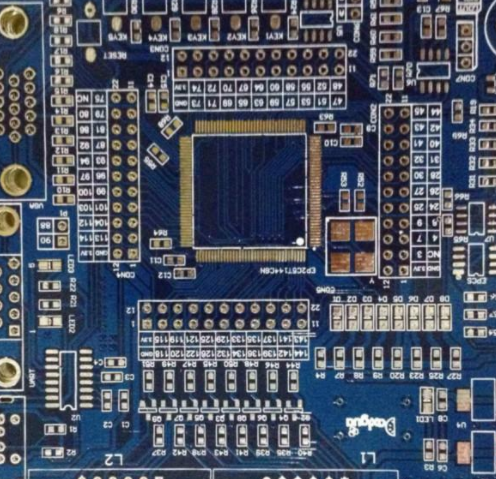
1. In the base plate, the pad of the DIE must be in the same direction as the binding line, and the outgoing line must also be in the same direction as the pad. For each DIE, a cross shaped pad must be placed at its diagonal position as the alignment coordinate during binding. This coordinate requires the network of connecting accessories, which is generally selected (there must be a network, otherwise the cross will not appear), In addition, in order to prevent the cross from being submerged by the copper sheet, which makes it impossible to locate accurately, it is generally surrounded by a copper plate frame.
2. The production process of the base plate is special. Each wire must be poured with copper material by electroplating to form bonding pads and wires, or all other places where copper is needed. It must be noted that even if there is no electrical connection or network for the pad, the pad must be pulled out of the board frame and copper plated in the eco mode, otherwise the pad will be copper free. In addition, the electroplating line pulled out of the plate frame must have a copper sheet on other layers to mark the corrosion position. Here, the seventh layer of copper sheet is used to mark the corrosion position. Generally speaking, the copper sheet is 0.15mm beyond the inside of the plate frame, while the edge of the copper sheet is about 0.2mm away from the plate frame.
3. To determine the positive and negative sides of the panel frame, it is better to place all components on the same side, which is marked with three XXX, as shown in the figure below.
4. The pad used for the base plate is larger than the general pad and has a special package, CX0201. The X mark is different from C0201. It is organized as follows:
0603 pad: 1.02mm × 0.92mm; the windowing area of pad: 0.9mmX0.8mm; the distance between two pads is 1.5mm.
0402 pad: 0.62mm × 0.62mm. The windowing area of the pad: 0.5mmX0.5mm. The distance between two pads is 1.0mm.
0201 pad: 0.42mm × 0.42mm. The windowing area of the pad: 0.3mmX0.3mm. The distance between two pads is 0.55mm.
5. The requirements for DIE are as follows: the minimum size of binding pad (single wire) is 0.2mmX0.09mm90 degrees, the minimum spacing between pads is 2MILS, and the width of the inner row of ground wire and power wire pads is also 0.2mm. The angle of binding pad shall be adjusted according to the angle of component cable. The binding wire is not easy to be too long when making the Substrate. The minimum distance between the master DIE and the inner bound pad is 0.4mm, and the minimum distance between the FLASHDIE and the bound pad is 0.2mm. The maximum length of the two binding wires should not exceed 3mm. The spacing between two rows of bonding pads shall be more than 0.27mm.
6. The distance between SMT pad and DIE binding pad as well as between SMT components shall be more than 0.3mm, and the distance between one DIE binding pad and another DIE shall also be more than 0.2mm. The minimum signal routing is 2 MILS, and the spacing is 2 MILS. The main power supply wiring should be 6-8 MILS, and the floor should be paved as large as possible. Power and other signal lines can be laid where the floor cannot be paved to enhance the strength of the substrate.
7. When wiring, pay attention to the vias and pads, routing, and gold fingers should not be too close. The vias with the same attributes and gold fingers should also be at least 0.12mm away, and vias with different attributes should be as far away from the pads and gold fingers as possible. The minimum through hole shall be 0.35mm for the outer hole and 0.2mm for the inner hole When laying copper, it should also be noted that the distance between the copper and the gold finger should not be very close. Some scrap copper should be removed, and no large area of copper is allowed to exist where the copper is not laid.
8. The grid shall be used when laying copper, and the proportion is 1:4, that is, the COPPERPOUR is 0.1mm and the COPPER is 0.4mm. The copper clad angle shall be changed to 45 degrees.
In this article, the inspection rules of PCB component layout and the design principles of PCB are mainly introduced.


