
Professional PCB manufacturing and assembly
Building 6, Zone 3, Yuekang Road,Bao'an District, Shenzhen, China
+86-13410863085Mon.-Sat.08:00-20:00

Mentor Rhine predicts PCB reorganization
San Jose, California? According to Worley Lane, CEO of Mentor Graphics, the circuit board tools department of EDA industry is now regarded as a mature, integrated and somewhat stagnant market, but it will become active soon In the keynote speech of the conference, PCB design Conference West held on Tuesday (March 16), it was predicted that with faster PCB design breaking the existing tools, users need to reorganize
"The complexity of integrated circuit design has expanded to the circuit board. You are reaching the limit of the chip level. Why not share the pain and make the circuit board design more complex? This is what is happening, but it is not linear. It occurs in an exponential form. It said that although most people are aware of the challenges of integrated circuit design tools, they do not know the" pressure "challenges faced by PCB design.
"EDA continues to add new functions to PCB tools to overcome the pressure, but the tools we provide are designed to a large extent a long time ago. I have an argument that printed circuit design will experience some very basic experience in integrated circuit design. Why.
PCB manufacturing, FPGA, signal integrity, library and data management and globalization are the five major pressures that will promote the near reorganization of PCB design.
PCB manufacturing is introducing new levels of complexity that tools cannot handle The use of micropores, high-density interconnects and embedded passive components has become more and more common He said that as designs become more complex, more and more of these technologies are used, and layout and cabling technologies may also be disturbed
He pointed out: "Compared with the method of only using laminated materials, users who use high-density interconnects (HDI) will benefit greatly if they can route on the pin density, take out from the package with high pin density, or reduce the wire spacing by five times." Microporous technology can save a lot of layers and density. With the development of new silicon technology, they will introduce more and more source devices. He said that PCB synthesis technology may be required to reduce the passive components in the design while maintaining the reduced shape factor space requirements.
Circuit board

As PCB design becomes more and more complex and FPGA becomes more and more popular, FPGA PCB design teams must work more closely to determine the trade-off between PCB and FPGA. Although this is not an imminent problem, technology that promotes communication between the two teams is needed to accelerate design and help the team work together.
In addition, signal integrity will remain unchanged. The chip and system speed continue to increase, and the circuit boards become more dense. 3GIO and asynchronous design are examples of fields that break the signal integrity rule of thumb and require "statistical analysis"
The related topics of library material management and globalization also indicate the breakthrough of current PCB design methods. With the development of new technologies and tools, libraries will also change, and companies need to be able to adapt to these changes.
"To some extent, the existing [library] format will be broken and moved, because they must have a new generation, they must be able to automate the part selection process, and integrate the EDA supplier library with the company's overall solution.
As teams from different parts of the world create more designs, they must use common libraries and data management software PCB companies can create software that allows design teams in different fields to design PCB at the same time
Common faults of PCB
Oct 21,2022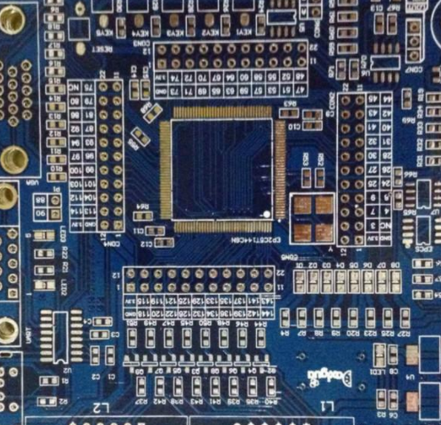


Just upload Gerber files, BOM files and design files, and the KINGFORD team will provide a complete quotation within 24h.