
Professional PCB manufacturing and assembly
Building 6, Zone 3, Yuekang Road,Bao'an District, Shenzhen, China
+86-13410863085Mon.-Sat.08:00-20:00

1. When designing the PCB layout, the design principle of placing it in a straight line along the signal flow should be fully followed, and try to avoid going back and forth.
Reason: To avoid direct coupling of signals and affect signal quality.
2. On the PCB board, the filtering, protection and isolation devices of the interface circuit should be placed close to the interface.
Reason: The effects of protection, filtering and isolation can be effectively realized.
3. If there are both filter and protection circuits at the interface, the principle of protection first and then filter should be followed.
Reason: The protection circuit is used for external overvoltage and overcurrent suppression. If the protection circuit is placed after the filter circuit, the filter circuit will be damaged by overvoltage and overcurrent.
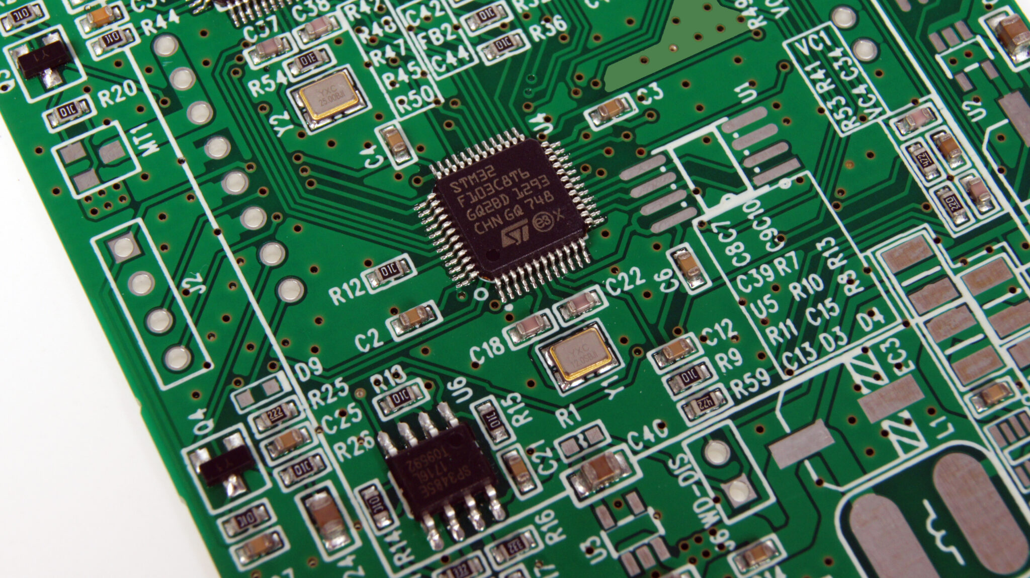
4. If the PCB clock frequency exceeds 5MHZ or the signal rise time is less than 5ns, multi-layer board design is generally required.
Reason: The signal loop area can be well controlled by using multi-layer board design.
5. For multi-layer boards, key wiring layers (clock lines, bus lines, interface signal lines, radio frequency lines, reset signal lines, chip selection signal lines, and various control signal lines) should be adjacent to the complete ground plane, preferably between two ground planes.
Reason: The key signal lines are generally strong radiation or extremely sensitive signal lines. Wiring close to the ground plane can reduce the area of the signal loop, reduce its radiation intensity or improve the anti-interference ability.
6. In a multi-layer board, the power plane should shrink 5H-20H relative to its adjacent ground plane (H is the distance between the power supply and the ground plane).
Reason: The retraction of the power plane relative to its return ground plane can effectively suppress the edge radiation problem.
7. In layered design, try to avoid the setting of adjacent wiring layers. If the adjacent wiring layers cannot be avoided, the layer spacing between the two wiring layers should be appropriately increased, and the layer spacing between the wiring layer and its signal loop should be reduced.
Cause: Parallel signal traces on adjacent routing layers can cause signal crosstalk.
8. Crystals, crystal oscillators, relays, switching power supplies and other strong radiation devices should be at least 1000mil away from the board interface connector.
Reason: The interference will directly radiate outward or couple the current on the outgoing cable to radiate outward.
9. Sensitive circuits or devices (such as reset circuits, WATCHDOG circuits, etc.) should be at least 1000mil away from the edges of the board, especially the edge of the interface side of the board.
Reason: Places like the board interface are the places most likely to be coupled by external interference (such as static electricity), and sensitive circuits such as reset circuits and watchdog circuits can easily cause system misoperations.
10. PCB traces cannot have right-angle or acute-angle traces.
Reason: Right-angle traces lead to impedance discontinuity, resulting in signal emission, resulting in ringing or overshoot, resulting in strong EMI radiation.
11. Try to avoid the layer setting of adjacent wiring layers. If it cannot be avoided, try to make the lines in the two wiring layers perpendicular to each other or the length of the parallel lines is less than 1000mil.
Reason: Reduce crosstalk between parallel traces.
12. Key signal traces such as clocks, buses, and radio frequency lines, and other parallel traces on the same layer should meet the 3W principle.
Reason: To avoid crosstalk between signals.
13. The key signal routing must not cross the partition area (including the reference plane gap caused by vias and pads).
Reason: Routing across partitions will increase the area of the signal loop.
14. When the signal line (especially the key signal line) changes layers, the ground via hole should be designed near the layer change hole.
Reason: It can reduce the signal loop area.
15. The key signal line is ≥3H from the edge of the reference plane (H is the height of the line from the reference plane).
Reason: Suppression of edge radiation effects.
16. For the grounding element of the metal shell, the grounding copper sheet should be laid on the top layer of its projection area.
Reason: The distributed capacitance between the metal shell and the grounding copper skin is used to suppress its external radiation and improve the immunity.


Just upload Gerber files, BOM files and design files, and the KINGFORD team will provide a complete quotation within 24h.