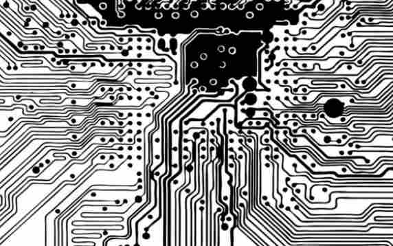
First, whether the design of rigid adagio need special design software and specifications? Domestic where can undertake this kind of circuit board processing?
Flexible Printed Circuit (PCB) can be designed with the general design of PCB software. Also use Gerber format for FPC manufacturers. Because the manufacturing process is different from ordinary PCBS, each manufacturer will have their own limits on minimum line width, minimum line spacing, and minimum aperture (via) according to their manufacturing capacity. In addition, the flexible circuit board can be strengthened by laying some copper around the bend. As for the manufacturer of the production can go online "FPC" when the keyword query should be found.
Second, what is the principle of the proper selection of PCB and shell grounding point?
The principle of PCB and case grounding selection is to provide a low-impedance returning current and controlling the returning current path using chassis ground. For example, the PCB floor can often be connected to the chassis ground by fastening screws near a high-frequency device or clock generator to minimize the overall current loop area, thus reducing electromagnetic radiation.
Three, circuit board debugging should start from what several aspects?
For digital circuits, first determine three things in order:
1. Ensure that all power supply values meet the design requirements. Some multi-power systems may require some specification of the order and speed at which certain power sources are connected.
2. Verify that all clock signal frequencies are working properly and that there are no non-monotonic issues on the edge of the signal.
3. Check whether the reset signal meets the specifications. If all this is normal, the chip should signal its first cycle. Next, debug according to the operating principle of the system and bus protocol.

Four, in the case of fixed circuit board size, if the design needs to accommodate more functions, it is often necessary to improve the PCB wire density, but this may lead to enhanced interference between the lines, at the same time, the fine line can not be reduced impedance, in the design of high speed and high density PCB, crosstalk interference is of particular concern because it has a significant effect on timing and signal integrity. Here are a few points to note:
1. Control the continuity and matching of the characteristic impedance of the cable.
2. Cable spacing. It is often seen that the spacing is twice the width of the line. Through simulation, we can know the influence of line spacing on timing and signal integrity, and find out the minimum tolerable distance. Different chip signals may have different results.
3. Select an appropriate terminal mode.
4. Avoid routing cables in the same direction or even overlapping on the upper and lower floors. This is because the cross-talk is greater than that on the same floors. 5. Use blind/buried via to increase cabling area. But the production cost of PCB board will increase. It's really hard to get exactly parallel and equal length in practice, but try to do it anyway. In addition, differential and common-mode terminations can be reserved to mitigate the impact on timing and signal integrity.
5. The filter at the analog power supply is often LC circuit. But why is LC sometimes less effective than RC?
The comparison of LC and RC filtering effect must consider whether the frequency band and inductance value to be filtered are appropriate. The value of reactance is related to the inductance value and frequency. If the noise frequency of the power supply is low and the inductance value is not large enough, then the filtering effect may not be as good as RC. However, the cost of using RC filtering is that the resistance itself consumes energy and has poor efficiency, and attention should be paid to the power that the selected resistance can withstand.
6. What is the method of choosing inductance and capacitance value when filtering?
In addition to the noise frequency filtered out, the response capacity of instantaneous current should be considered in the selection of inductance value. If the output end of LC has the chance to output a large current instantaneously, the inductance value is too large to hinder the speed of the large current flowing through the inductance, and increase the ripple noise. The capacitance value is related to the standard value of ripple noise that can be tolerated. The smaller the ripple noise value is, the larger the capacitance value will be. The ESR/ESL of capacitors also has an effect. In addition, if the LC is placed on the output end of the switching regulation power, it is necessary to pay attention to the pole/zero generated by the LC on the stability of the negative feedback control loop.


