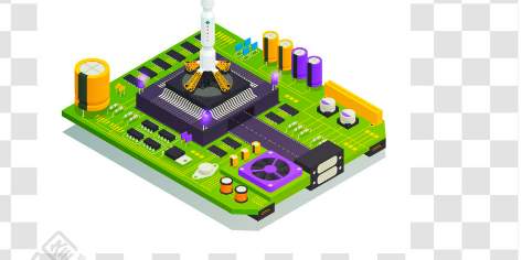
1. PCB design of process equipment
Device layout requirements
Component layout should be neat and beautiful, the same type of components should be integrated
▪ Based on the direction of over-wave soldering (reflow soldering) of PCB, the spacing between the front and rear plates of any component or its body should be more than 4.0mm, and the spacing between the left and right plates should be more than 5.0mm; Otherwise, a process edge must be added. To facilitate processing and transportation.
▪ The layout of printed circuit boards using automatic plug-in technology should meet the technical requirements of automatic plug-in machines.
Two, the placement of components should consider the height of components, component layout should be uniform, compact, beautiful, balanced center of gravity, and must ensure installation.
▪ The location of components should be at the grid points recommended by the circuit design software (2.54mm).
▪ The spacing between any component body should be at least 0.5mm, at least not close together. To prevent the component is difficult to plug in place or unfavorable heat dissipation.
▪ Considering the convenience of assembly, production line maintenance and after-sales service maintenance, the socket design of external parts is easy to plug in the position, the selection of the socket and the color of the socket can be distinguished to ensure that there will be no mistakes in plugging.
▪ Component layout should be matched with electric control box assembly. Tall components, especially pin relay, fan capacitor, strong electric socket, high-power raising resistance, mutual inductance, etc. should have a gap between the highest point and the box body after assembly into the electric control box, so as to affect the smooth assembly and stress, resulting in reduced reliability of electric control.

▪ The plugging action of connectors should be smooth and the socket should not be too close to other components.
▪ Component layout should consider the balance of the center of gravity. The center of gravity of the entire board should be close to the geometric center of the PCB. The center of gravity should not be allowed to drift to the edge of the board (1/4 area).
Three, plug-in, welding and material turnover quality requirements for PCB design device layout
The different requirements for the device layout are put forward in the aspect of quality.
▪ Similar components are oriented in the same direction on the circuit board (e.g. diodes, leds, electrolytic capacitors, receptacles, etc.) so that plug-ins are errless, beautiful and productive.
▪ Horizontal design should be adopted for 220 package regulator tubes (especially those close to the edge of the plate), such as 7805/7812, which do not need heat sink, in order to prevent the element foot or copper skin from being broken by external forces during the process and transfer, handling, inspection and assembly.
▪ Metal-clad crystals, designed as horizontally as possible to withstand shocks and secured with glue.
▪ The orientation of the long axis of the patch element (especially the thicker patch element) should be as perpendicular as possible to the forward direction of wave soldering to avoid shadow areas as far as possible.
▪ As far as dual panels are concerned: SMT components for the solder paste process are prefered to be designed on the plug-in component surface, while for the red glue process, the plate is designed on the wave soldering surface as far as possible.
For patch components. The spacing between adjacent components and pads should not be too close. It is recommended to design according to the following principles.
(1) The distance between PLCC, QFP and SOP and each other is not less than 2.5mm.
(2) The spacing between PLCC, QFP, SOP and Chip and SOT is not less than 1.5 mm.
(3) Spacing between Chip and SOT ≥ 0.7mm.
▪ Multi-core socket, connecting wire group, foot spacing intensive double row foot manual plug-in IC, the long side direction must be parallel to the direction of the wave crest, and the front and back of the most next to the foot to increase the false pad or increase the area of the original pad, in order to absorb the trailing solder to solve the welding problem. As shown below:
▪ If the OFP and PLCC integrated blocks pass the crest by red glue process, they should be placed at a 45 degree bevel, and the last pin of each side should be added with a stolen tin pad;
Iv. Creepage distance and electrical clearance shall meet the requirements of GB4706.1-1998.
▪ When 130V < operating voltage ≤250V, no anti-dust ability conditions, electrical insulation gap between different phases ≥2.5mm, creepage distance ≥3.0mm, basic insulation (between strong and weak electricity) electrical gap ≥3.0mm, creepage distance ≥4.0mm, groove width should be greater than 1mm, the length of the groove should ensure creepage distance meet requirements.
5. Device layout shall meet the requirements of fire protection design specifications.
▪ The heat dissipation effect of high-power components must be considered, and must be placed in a position with good heat dissipation effect.
▪ There should be a gap of more than 2mm between the high-power resistor body and the surrounding components body. In principle, the high-power resistor should be designed in elevated horizontal mode. .
Vi. Device layout shall meet the requirements of EMC design specifications.
▪ Cell circuits should be placed as close together as possible.
▪ Devices sensitive to temperature characteristics should be kept away from power devices.
▪ Key circuits, such as reset and clock devices, should be kept away from high-current circuits.
▪ The decoupling capacitor should be close to its power supply circuit.
▪ The circuit area should be minimum.


