
Professional PCB manufacturing and assembly
Building 6, Zone 3, Yuekang Road,Bao'an District, Shenzhen, China
+86-13410863085Mon.-Sat.08:00-20:00

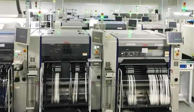
1. Substrate transmission system: transmission guide rail, PCB in, stop and move out functions.
2. PCB positioning system: working platform, PCB fixing, support, release fixing.
3. Device feeding system: the feeding function of the feeding platform and the feeder patch device.
4. Visual identification system: PCB camera, component camera, center compensation function.
5. Mount control system: mount head, take material, X/Y/R/Z axis movement, mount function.
6. CPU control system: control box drive, servo, vision, computer control card.
placement machine works
1. Function of the SMT machine: place the electronic components on the PCB according to the correct position and Angle.
2. Placement machine programming: placement action requires program instructions. Programming requires BOM, coordinate file, polarity indication.
SMT machine processing capacity (different models of SMT machine have differences)
1. PCB size: L50*W50mm ~ L510*W460mm, T=05 ~ 4.0mm.
2. Component size: 03015mm ~ W55*L100mmH=15mm.
3. The minimum spacing is 03mm and the minimum electrode size is 017mm.
4. The element type: Chip/SOT/PT/SOP/QFP/BGA/DFN/CON, etc.
5. Packing: TapeReel, Tray, tube packing (not recommended).
6. Material type: braid according to 8mmFeeder, 20 ~ 100 kinds, Tray15 kinds, can be more than one patch unit, improve the type of material installation.
7. Patch speed: theoretical points 20000 ~ 200000CPH, the actual efficiency between 45% ~ 75%, can be multiple patch unit combined to improve production efficiency.

Type of component
Patch component dimensions
Unit size conversion in imperial system (0.12 inch =120mi1, 0.08 inch =80mi1)
device placement for manufacturability design requirements
1. PCB size conforms to the SMT machine processing capacity size is insufficient, need to assemble the board, the size of the board cannot be greater than the specifications of the SMT machine.
2. The selection of components conforms to the processing capability of the SMT machine, and gives priority to the selection of conventional types, reducing the requirement of accuracy and enlarging the process window.
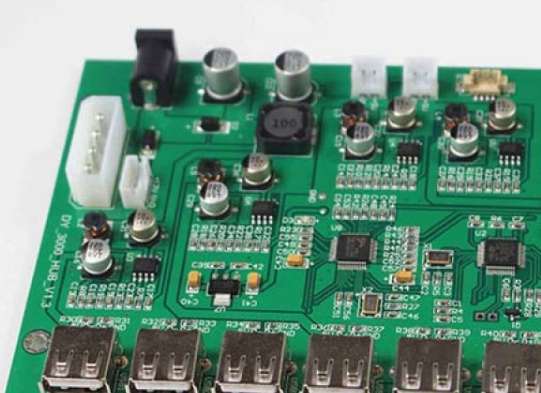
3. PCB pad design shall meet the requirements of IPC-SM-782, and device packaging and pad design and packaging shall be fully matched.
4. PCB design shall clearly mark the position number, positive and negative poles and polarity with silk screen, or provide drawings without ambiguity.
5. Provide the BOM coordinate file and drawings correctly (if the PCB silkscreen is not clear, provide them).
BOM clearly expresses the component name, package size, material specifications, parameters, attributes, dosage, and location number.
Coordinate files need to have X, Y, R, position number, package size, B/T level.
The drawing should clearly indicate the position number, positive and negative poles, and the polarity symbol (pin 1). The polarity symbol should be consistent with the device.
6. Materials are packed in a braided Tray. Tubular packing is not recommended. Class B and C materials must be damaged; Coplanar properties of pin devices.
7. In order to improve the production efficiency, it is recommended to fit the board with a small number of patch components.
8. PCB design device minimum clearance greater than 0.3mm.
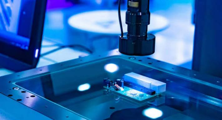
AOI: furnace AOI automatic optical inspection, through the CCD camera image, then through processing is the intelligent application of specially software (according to the pixel distribution, brightness and color information, such as converted into digital signals) into the information we need. AOI system test process is mainly through the image of the component to be tested and the standard image comparison to determine whether the component is OK, including the component size, Angle, offset, position and character, mainly for the following bad: wrong parts, missing parts, polar reverse, offset. Intercept the defective devices before welding to avoid the increase of maintenance cost and scrap risk after the defective mounting devices enter reflow welding.
Reflow Soldering, a literal translation of the English Reflow soldering, is the welding of mechanical and electrical connections between the solder ends or pins of the surface-assembled components and the printed board pad by melting the solder paste printed onto the pad. reflow soldering
a) Infrared welding
b) Infrared + Hot air (combination)
c) Gas phase welding (VPS)
d) Hot air welding is currently commonly used
e) Hot core plate (rarely used)
reflow soldering process
1. Preheating: PCB and components preheat to reduce thermal shock.
2. Hot core plate (rarely used) constant temperature: flux dissolution, cleaning pad, components, tin powder surface oxide, too much volatile flux; PCB temperature and component visibility reach equilibrium.
3. Reflux: the metal component in the solder paste melts the wetting element Lead, and begins to form the alloy layer.
4. Cooling: The temperature is quickly reduced to below the melting point, forming a solid solder joint.
reflow soldering equipment capability
1. Temperature stability +5℃ deviation, adjustable precision 1℃ or 0.1℃.
2. There are 8, 10 and 12 warm zones up and down.
3. Temperature difference range The maximum temperature difference between adjacent temperature zones and upper and lower temperature zones can be set without cross-temperature.
4. Thermal compensation capacity for large heat absorption PCBA or use of vehicle through the furnace, rapid temperature compensation and constant temperature capacity.
5. Permissible broadband error range of track parallel capability.
6 track and network belt transmission temperature stable transmission, no jitter.
7. Sealing performance of furnace reflow welding to the external heat dissipation, shell temperature.
reflow soldering for manufacturability design requirements
1. PCB substrate selection to withstand temperature above 265℃ requirements:
2. The temperature resistance of all patch devices can reach 265℃ for 5 seconds.
3. Temperature and humidity sensitive devices, such as IC and LED lamps (level3 level 4), must be stored in vacuum or moisture-proof.
4. PCB surface treatment, PAD width is less than 0.2mm, BGA PAD diameter is less than 0.5mm.
5. 0201 and below pads are not suitable for tin-spraying process, recommended gold plating and OSP process.
6. The distance between PCB pads is greater than 0.15mm.
7. Components with large weight and high height are recommended to be placed on the TOP side of PCB design.
8. The PAD surface shall not have VIA holes, and the PAD size of the components shall be symmetrical.
9. The inner spacing of PCB design component library PAD conforms to IPC-SM-782 standard.
10. The PAD is a large ground pad and needs to be divided into fancy or cross connections.


Just upload Gerber files, BOM files and design files, and the KINGFORD team will provide a complete quotation within 24h.