
Professional PCB manufacturing and assembly
Building 6, Zone 3, Yuekang Road,Bao'an District, Shenzhen, China
+86-13410863085Mon.-Sat.08:00-20:00

PCB dead copper is also called PCB island, refers to the isolated copper foil without connection in PCB, generally generated when laying copper, the PCB design should remove dead copper?
Some people say it should be removed, probably for the following reasons:
1. EMI problems may be caused.
2, enhance anti-interference ability.
3. Dead copper is useless.
Some people say it should be kept, probably for the following reasons:
1, go to sometimes large blank does not look good.
2, increase the mechanical properties of the board, avoid the phenomenon of uneven bending.
Should PCB design remove dead copper?
Next, kingford, a professional PCB design company in Shenzhen, will introduce you in detail:
First, we don't want to die copper (island), because the island here forms an antenna effect, if the radiation intensity of the surrounding line is high, it will enhance the radiation intensity of the surrounding; And will form the antenna acceptance effect, will introduce electromagnetic interference to the surrounding lines.
Second, we can delete some small islands. If we wish to retain the copper cladding, the island should be well connected to GND through the ground hole to form a shield.
Third, in the case of high frequency, the distributed capacitance of the wiring on the printed circuit board will play a role. When the length is greater than 1/20 of the wavelength corresponding to the noise frequency, the antenna effect will be generated, and the noise will be emitted outward through the wiring. If there is a bad grounded copper coating in the PCB, the copper coating will become a tool to propagate the noise. The ground ground to a certain place, this is the "ground wire", must be less than λ/20 spacing, in the wiring through the hole, and the ground plane of the multilayer "good grounding". If the copper coating is properly treated, the copper coating not only increases the current, but also plays the dual role of shielding interference.
Fourth, by punching the ground hole, to retain the island of copper cover, not only can play the role of shielding interference, indeed can also prevent PCB deformation.
kingford PCB design capability:
Maximum signal design rate: 10Gbps CML differential signal;
Maximum number of PCB design layers: 40;
Minimum line width: 2.4mil;
Minimum line spacing: 2.4mil;
Minimum BGA PIN spacing: 0.4mm;
Minimum mechanical hole diameter: 6mil;
Minimum laser drilling diameter: 4mil;
Maximum number of pins:; 63000 +
Maximum number of components: 3600;
Maximum number of BGA: 48+.
PCB design service process
1. The customer provides schematic diagram to consult PCB board design;
2. Evaluate quotation according to schematic diagram and customer design requirements;
3. The customer confirms the quotation, signs the contract and pays the project deposit;
4. Received advance payment and arranged engineer design;
5. After the design is completed, provide the screenshot of the document to the customer for confirmation;
6. The customer confirmed OK, settled the balance, and provided PCB design materials.
2. Points for attention in DC-DC circuit PCB design
Compared with LDO, the PCB design of DC-DC circuit will be much more complex, with greater noise and higher requirements for layout and layout. The quality of layout directly affects the performance of DC-DC, so it is very important to understand the layout of DC-DC.
First, Bad layout
- EMI, DC-DC SW pin will have a higher dv/dt, a higher dv/dt will cause more EMI interference;
- Ground noise. Poor ground wiring will generate large switching noise above the ground wire, which will affect other parts of the circuit;
- There will be voltage drop on the wiring. If the wiring is too long, the voltage drop will be generated on the wiring, and the efficiency of the whole DC-DC will be reduced.
Ii. General Principles
- Switch large current circuit as short as possible;
- The signal ground and the high-current ground (power ground) are routed separately and connected in a single point at the chip GND;
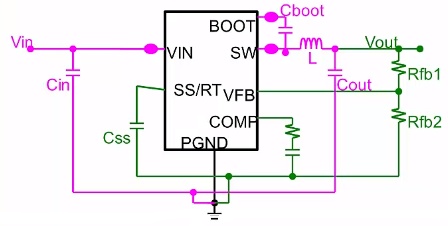
1. The switching loop is short
The red LOOP1 in the figure below is the current flow direction when the DC-DC high-side pipe is on and the low-side pipe is off. Green LOOP2 is the current flow direction when the high side pipe is closed and the low side pipe is opened;
In order to make the two loops as small as possible and introduce less interference, the following principles need to be followed:
- Inductance as close to SW pin as possible;
- Input capacitance as close to VIN pin as possible;
- The ground of the input and output capacitor is close to the PGND pin as far as possible;
- Use copper laying mode for wiring;
DC-DC PCB design
Why would you do that?
- Too fine and too long wire running will increase the impedance, and a large current will produce a relatively high ripple voltage in this large impedance;
- Too long and too thin wire running will increase the parasitic inductance, and the coupling switch noise on this inductance will affect the stability of DC-DC and cause EMI problems;
- Parasitic capacitance and impedance will increase switching loss and on-off loss, affecting DC-DC efficiency;
2. Single point grounding
Single point grounding refers to the single point grounding between signal ground and power ground. There will be relatively large switching noise on power ground, so it is necessary to avoid causing interference to sensitive small signals, such as FB feedback pin.
- High current: L, Cin, Cout, Cboot connect to the network of high current ground;
- Low current ground: Css, Rfb1, Rfb2 separately connected to the signal ground network;

Iii. Examples
The layout of a typical DC-DC BUCK circuit is given below, and the following points are given in the SPEC:
- Input capacitors, high-edge MOS tubes, and relays form switching loops that are as small and short as possible;
- Input capacitor as close as possible to Vin Pin pin;
- Ensure that all feedback connections are short and direct, and feedback resistors and compensating elements are as close to the chip as possible;
- SW is far away from sensitive signals, such as FB;
- Connect VIN, SW, and especially GND separately to a large copper area to cool the chip and improve thermal performance and long-term reliability;
Iv. Summary
layout of DC-DC circuit is very important, which directly affects the working stability and performance of DC-DC. Generally, SPEC of DC-DC chip will give layout guidance, which can be referred to for design.


Just upload Gerber files, BOM files and design files, and the KINGFORD team will provide a complete quotation within 24h.