
Professional PCB manufacturing and assembly
Building 6, Zone 3, Yuekang Road,Bao'an District, Shenzhen, China
+86-13410863085Mon.-Sat.08:00-20:00

The design of the printed circuit board is based on the schematic diagram of the circuit to achieve the function required by the circuit designer. The design of printed circuit board mainly refers to the layout design, which needs to consider the layout of external connections, the optimal layout of internal electronic components, the optimal layout of metal wires and through holes, electromagnetic protection, heat dissipation and other factors. Excellent layout design can save production cost, achieve good circuit performance and heat dissipation performance. Simple layout design can be realized by hand, complex layout design needs to be realized by computer aided design (CAD).
1. Ground wire design
In electronic equipment circuit board, circuit board, PCB board, grounding is an important method to control interference. If the grounding and shielding can be correctly combined, most interference problems can be solved. The structure of ground wire in electronic equipment is generally systematic, housing ground (shield ground), digital ground (logic) and simulation ground. The following points should be noted in the design of ground wire:
(1) Correctly select single point grounding and multi-point grounding.
In low-frequency circuit, the working frequency of signal is less than 1MHz, and the inductance between wiring and devices has little influence, while the circulation formed by grounding circuit has great influence on interference, so one-point grounding should be used. When the signal working frequency is greater than 10MHz, the ground impedance becomes large. In this case, the ground impedance should be reduced as much as possible and the nearest multipoint grounding should be used. When the operating frequency ranges from 1 MHZ to 10 MHZ, if a one-point grounding is used, the length of the ground wire should not exceed 1/20 of the wavelength. Otherwise, the multi-point grounding method should be used.
(2) Separate the digital circuit from the simulation circuit
Both high-speed logic circuit and linear circuit on the circuit board should be separated as far as possible, and the ground wire of the two should not be mixed, respectively connected with the ground wire of the power supply end. The ground area of the linear circuit should be increased as much as possible.
(3) Make the ground cable as thick as possible
If the grounding wire is very thin, the grounding potential will change with the change of the current, resulting in the timing signal level of the electronic equipment is unstable, and the anti-noise performance becomes worse. The ground wire should therefore be made as thick as possible so that it can pass through three times the allowable current of the printed circuit board. If possible, the ground cable should be wider than 3mm.
(4) The ground wire is formed into a dead-cycle road
When designing the ground system of printed circuit board composed only of digital circuit, making the ground wire into a dead-cycle circuit can obviously improve the anti-noise ability. The reason is that there are many integrated circuit components on the printed circuit board, especially in the case of power consumption of components, due to the limitation of the thickness of the grounding wire, will produce a large potential difference on the ground junction, causing the decrease of anti-noise ability, if the grounding structure into a loop, it will reduce the potential difference, improve the anti-noise ability of electronic equipment.
2. High-speed multilayer
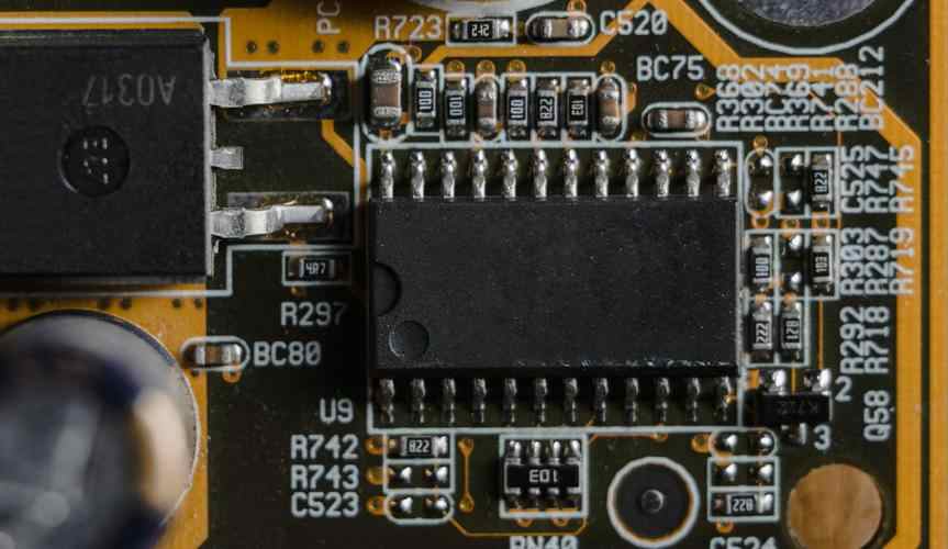
In electronic products tend to be multifunctional and complex under the preceding problem, the contact distance of integrated circuit components is reduced, the speed of signal transmission is relatively improved, followed by the increase in the number of wiring, the length of the local shortening between the points, which requires the application of high-density line configuration and microporous technology to achieve the purpose. Wiring and crossover basically for single and double panel has its difficulties, so the Circuit Board will move to Multilayer, and because of the continuous increase of signal lines, more power layer and ground is a must for the design, these make the Multilayer Printed Circuit Board (printed circuit board) more common.
For the electrical requirements of high-speed signals, the circuit board must provide impedance control with alternating current characteristics, high frequency transmission capability, reduce unnecessary radiation (EMI), etc. With the structure of Stripline and Microstrip, multilayer design becomes necessary. To reduce signal transmission quality problems, insulation materials with low dielectric coefficient and low decay rate are used. In line with the miniaturization and array of electronic components, the density of circuit boards is constantly increased to meet demand. The appearance of BGA (Ball Grid Array), CSP (Chip Scale Package), DCA (Direct Chip Attachment) and other groups of parts assembly mode, more promote the printed circuit board to the unprecedented high density.
Any hole with a diameter of less than 150um is called Microvia in the industry. The circuit made by using the geometric structure technology of this microhole can improve the efficiency of assembly, space utilization and so on. At the same time, it is also necessary for the miniaturization of electronic products.
For this kind of structure of the circuit board products, the industry has a number of different names to call this circuit board. For example, European and American manufacturers used to call this kind of product SBU (Sequence Build UpProcess), which is generally translated as "sequence build upprocess", because the production process is built in sequence. As for the Japanese, the manufacturing technology of this kind of product is called MVP (Micro Via Process), which is generally translated as "microporous process", because the pore structure of this kind of product is much smaller than the previous ones. Because the traditional Multilayer Board is called MLB (Multilayer Board), some people call this kind of circuit board BUM (Build Up Multilayer Board), which is generally translated as "addition-layer multilayer board".
Method of removing integrated circuit board
Feb 12,2023


Just upload Gerber files, BOM files and design files, and the KINGFORD team will provide a complete quotation within 24h.