
Professional PCB manufacturing and assembly
Building 6, Zone 3, Yuekang Road,Bao'an District, Shenzhen, China
+86-13410863085Mon.-Sat.08:00-20:00

Chengdu Zicheng Electronics is a professional PCB design company engaged in electronic products circuit board design (layout and wiring design). Mainly undertake multi-layer, high density PCB design drawing board and circuit board design proofing business. Next, I will share with you the golden rules of PCB wiring.

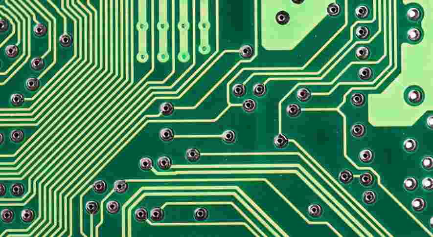
PCB routing is the layout of the printed circuit according to the PCB circuit schematic, line table and the required line width and spacing. Wiring should generally follow the following rules:
1, under the premise of meeting the requirements of use, wiring as simple as possible. The order of selecting wiring mode is single-layer - double-layer - multilayer.
2. The wiring between the two patch joints should be as short as possible. Sensitive signals and small signals should go first to reduce the delay and interference of small signals. The ground shield should be arranged next to the input line of the analog circuit; The layout of the same layer wire should be evenly distributed; The conductive area of each layer should be relatively balanced to prevent the circuit board from warping during pcba processing.
3, signal line change direction, should be along the diagonal or smooth transition, curvature radius should be large, to avoid electric field concentration, signal reflection and additional impedance.
4, digital circuit and analog circuit wiring should be separated to avoid mutual interference. If they are on the same floor, the cables for the ground system and the power system should be laid separately. Ground wires are separated to avoid crosstalk. In order to facilitate testing, the design should set the necessary breakpoints and test points.
5, circuit components should be grounded, and as short and close to the power supply as possible, in order to reduce internal resistance.
6. The upper and lower layers should be perpendicular to each other to reduce coupling. The upper and lower layers should not be aligned or parallel. Reasonable wiring layout in PCB patch processing can not only reduce the defective rate of products, but also improve the pass rate.
7. Multiple I/O lines of high-speed circuits and I/O lines of differential amplifiers, balance amplifiers and other circuits should be equal in length to avoid unnecessary delay or phase shift.
8. When pcb welding pad is connected to a large conductive area, a thin wire with a length of no less than 0.5m should be used for thermal isolation, and the width of the thin wire should not be less than or greater than 0.13mm.
8. The nearest cable is at least 5mm away from the SMB edge. If necessary, the ground cable can be close to the SMB edge. If a rail is to be inserted during SMT processing, the distance between the wire and the SMB edge should be at least greater than the groove depth of the rail.
9. The public power cables and ground cables on the double-sided SMB should be arranged as close to the edge of the SMB as possible and distributed on both sides of the SMB. The power layer and ground cable layer can be installed at the inner layer of the multi-layer SMB, and are connected to the power cables and ground cables at each layer through metallic holes. Improve the cohesion between the multiple SMB layers.
Why should the high reliability of PCB be taken seriously?
High reliability is a practical science combining "engineering technology" and "management art". To produce high reliability PCB stably, a set of "standardized, efficient, collaborative and controllable" management procedures must be established. A series of influencing factors such as engineering design, production materials, manufacturing equipment, process, quality assurance facilities, production environment, management system and team quality are required to be fully controlled by the factory.
Therefore, to evaluate whether the PCB has "high reliability", we need to deeply confirm whether the following control items of the factory have been fully controlled.
01 Prevention Mechanism
1) Engineering design: customer requirement identification, information management, automatic operation, professional skills; Design standard specifications that modify manufacturability based on factory process capabilities; Work specification, process standardization, engineering automation;
2) Manufacturing process: systematic and systematic management of the control objectives, operating procedures and operation specifications of each process of the whole process;
As the carrier of various electronic components and the hub of circuit signal transmission, PCB determines the quality and reliability of electronic packaging. With the increasing miniaturization, lightweight and multi-function of electronic products, as well as the continuous promotion of environmental protection requirements such as lead-free and halogen free, PCB industry is showing a development trend of "thin line, small hole, multiple layers, thin board, high frequency and high speed", and the requirements for reliability will be higher and higher.
High reliability PCB can play the role of robust carrier, realize the long-term and stable operation of PCBA, so as to ensure the safety, stability and service life of terminal products, and enterprises can enhance competitiveness, enhance reputation, expand market share, and improve economic benefits.


Just upload Gerber files, BOM files and design files, and the KINGFORD team will provide a complete quotation within 24h.