
Professional PCB manufacturing and assembly
Building 6, Zone 3, Yuekang Road,Bao'an District, Shenzhen, China
+86-13410863085Mon.-Sat.08:00-20:00

At present, the integrity of high speed circuit power supply faces various challenges, such as higher and higher chip integration of low voltage power supply, development of PCB design to high speed and high density, increasing difficulty of PDN decoupling capacitor optimization, and electrothermal collaborative analysis of large current. In order to ensure the stable operation of the system, provide stable power supply and current for the chip, improve the quality of the power supply, reduce the overall power impedance of the system, and improve the reliability and stability of the product. The trend of integrated circuits along Moore's Law presents increasing challenges for power distribution network (PDN) design and power integrity (PI) analysis of contemporary electronic systems:
1. Chip integration of low voltage power supply is getting higher and higher
The lower the voltage, the greater the current required on each device pin, resulting in a larger DC voltage drop. The lower the voltage, the more stringent the requirement to control the voltage drop. The typical voltage requirement is usually ±5%, which means that the allowed DC voltage drop is smaller. The more integrated the device, the denser the wiring around the integrated circuit, resulting in a higher current density in the power network and a larger DC voltage drop.
2.PCB design develops to high speed and high density
Nowadays, the space on PCB boards is getting smaller and the signal routing is getting denser, and there are not many places for a spacious power plane. As a result, both the power plane and the ground plane are penetrated by backpads around other network through-holes. Since there are many holes in the layer, it is obvious that the path available for current flow becomes thinner, so the resistance of the power plane becomes larger, resulting in a larger DC voltage drop.
3.PDN decoupling capacitor optimization is more difficult
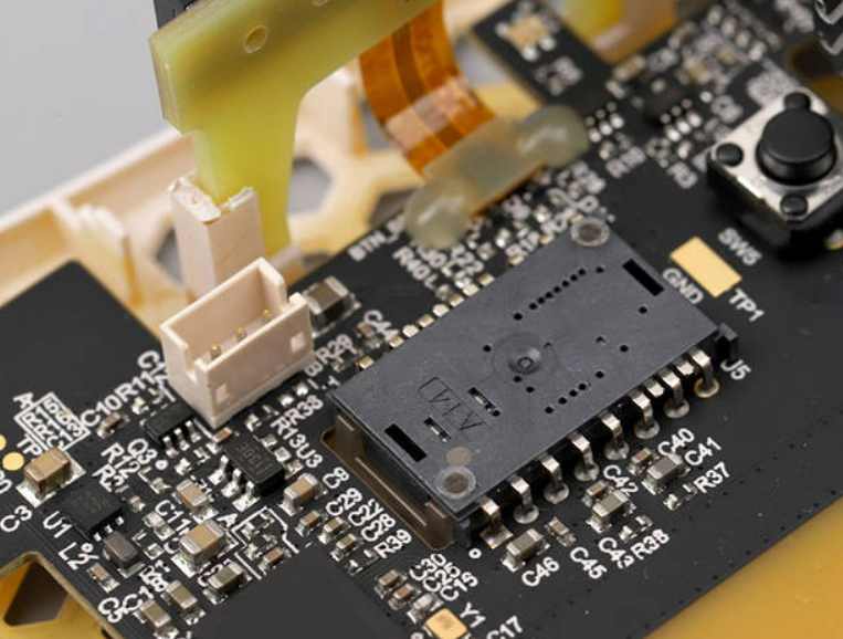
In high speed PCB design, decoupling capacitor plays an important role, and its placement is also important. This is because when the power supply is supplied to the load for a short time, the stored charge in the capacitor can prevent voltage drop. If the capacitor is placed improperly, the line impedance will be too large, affecting the power supply. At the same time, the capacitor can filter out the high-frequency noise when the device is switched at high speed. In our high-speed PCB design, we generally add a decoupling capacitor at the output end of the power supply and the input end of the power supply of the chip. The capacitance value near the power supply is generally large (such as 10μF). This is because we generally use a DC power supply in PCB, and the resonant frequency of the capacitor can be relatively low in order to filter the noise of the power supply. At the same time, large capacitance can ensure the stability of power output. For the decoupling capacitor added to the pin of the chip connected to the power supply, its capacitance value is generally small (such as 0.1μF), because in the high-speed chip, the noise frequency is generally relatively high, which requires the resonant frequency of the decoupling capacitor to be high, that is, the capacitance value of the decoupling capacitor to be small.
The PDN system of the power supply requires that each system component can get the normal operating voltage, so it is necessary to carry on the impedance control of the power supply. As long as the power impedance is controlled below the target impedance, the voltage transmission will have a good performance guarantee. However, in the actual design, a large number of decoupling capacitors are connected to PDN. They are the most important part of PDN, which almost determines the quality of PDN. How many capacitors does PDN need to effectively suppress noise? Where are these capacitors placed? How to install? On the basis of ensuring good performance of the power supply, how to reduce the tension of PCB layout by reducing the capacitance, and thus save the design cost is a big challenge for the integrity analysis of the power supply.
4. Electrothermal collaborative analysis under large current
As the chip integration becomes higher and higher, the power supply current of the chip power supply increases and the power loss on the passive link increases. The loss of this part will be presented in the form of heat, thus leading to thermal design risk. Meanwhile, the passive link will also be affected by temperature, so the electrothermal cooperative analysis of large current is particularly important.
The high-speed system design and simulation product line provides a simulation platform for rapid modeling and passive parameter extraction of PCB board, component and system interconnection structure, and solves the problem of signal and power integrity in high-speed and high-frequency systems.
Chip design and packaging and PCB
Feb 10,2023


Just upload Gerber files, BOM files and design files, and the KINGFORD team will provide a complete quotation within 24h.