
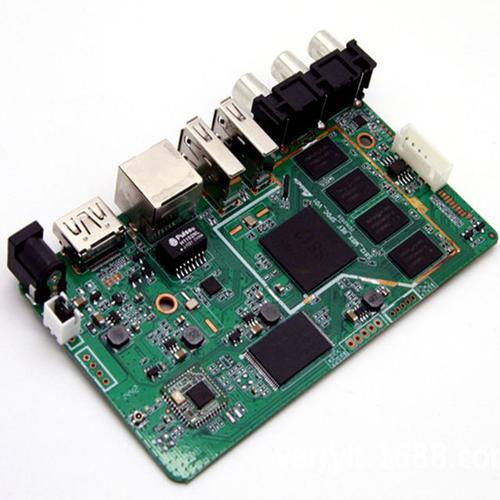
Professional PCB manufacturing and assembly
Building 6, Zone 3, Yuekang Road,Bao'an District, Shenzhen, China
+86-13410863085Mon.-Sat.08:00-20:00

One, layer distribution
1. Dual panels: the top layer is the signal layer, and the bottom surface is the ground plane.
2. Four-layer board, the top layer is the signal layer, the second layer is the ground plane, and the third layer is the power supply and control line. In special cases (for example, the RF signal cables pass through the shielding wall), some RF signal cables should be routed at the third layer. Each layer requires a large area of ground.
Two, grounding
1. Large area grounding To reduce the ground plane impedance and achieve good grounding effect, you are advised to comply with the following requirements: (1) RF PCB grounding requires large area grounding; (2) In the microstrip printed circuit, the bottom surface is ground, which must be smooth and smooth; (3) to the contact surface of the ground gold-plated or silver-plated, good conduction, in order to reduce the grounding resistance; (4) Use the fastening screw, so that it is closely combined with the shielding cavity, fastening screw spacing is less than λ/20 (depending on the specific situation).
2. Grouping nearby grounding The whole circuit is divided into several relatively independent groups according to the structure distribution of the circuit and the size of the current. Each group of circuits forms a circuit on the near grounding. Note that the ground wire should be short and straight, do not overlap, reduce the interference caused by the common ground impedance.
3. When the grounding surface of the RF device is attached to the RF device and the filter capacitor need to be grounded, in order to reduce the grounding inductance of the device, the following requirements are required: (1) At least two wires must be connected to the ground copper foil; (2) Ground at least two metallized holes near the pin of the device. (3) Increase the aperture of the through hole and parallel several through holes. (4) The bottom of some components is a grounded metal shell, to add some ground holes in the projection area of the components, the surface layer shall not be wired.

4. Grounding of microstrip circuit microstrip printed circuit terminal single grounding hole diameter must be greater than the microstrip line width, or the terminal a large number of rows of holes.
4. Requirements for grounding technology
(1) The distance between the pad and the hole can be shortened if the process allows;
(2) If the process permits, the large grounded pad can be directly covered on at least 6 grounding holes (the specific number varies with the size of the pad);
(3) When the ground wire needs to go a certain distance, the length of the wire should be shortened, and more than λ/20 is prohibited, so as to prevent signal radiation caused by antenna effect;
(4) Except for special purposes, there shall be no isolated copper foil, copper foil must be added ground wire hole;
(5) It is prohibited to extend the wire head of the open terminal on the copper foil of the ground wire.
Three, shielding
1. Radio frequency signals can radiate in the air medium. The larger the space distance, the lower the operating frequency, the smaller the host coupling and the greater the isolation degree. PCBS typically have a spatial isolation of about 50dB.
2 sensitive circuit and strong radiation source circuit to add shielding, but if the design and processing is difficult (such as space or cost limit system, etc.), do not add, but to do the test final decision. These circuits are:
3. The front end of the receiving PCB circuit board is a sensitive circuit, and the signal is very small, so it should be shielded.
4. The radio frequency unit and intermediate frequency unit must be shielded. The IF signal of the receiving channel will cause great interference to the RF signal; conversely, the RF signal of the transmitting channel will also cause radiation interference to the IF signal.
5. Oscillation circuit: strong radiation source, the local vibration source should be screened separately, due to the high level of the local vibration, the radiation interference to other units will be larger.
6 power amplifier and day feed circuit: strong radiation source, strong signal, to shield.
7. Digital signal processing circuit: strong radiation source, high speed digital signal steep up and down will interfere with analog radio frequency signal.
8. Cascade amplifier circuit: the total gain may exceed the spatial isolation degree from the output to the input, so that one of the oscillation conditions is satisfied, and the circuit may be self-excited. If the in-frequency gain of the circuit in the cavity exceeds 30-50dB, a metal shield plate must be welded or installed on the PCB board to increase the isolation. In the actual design, the frequency, power and gain should be considered comprehensively to decide whether to add shielding plate.
9. Cascaded filter, switch, attenuation circuit: in the same shielding cavity, the out-of-band attenuation of the cascaded filter circuit, the isolation of the cascaded switch circuit, the attenuation of the cascaded attenuation circuit must be less than 30-50dB. If this value is exceeded, a metal shield plate must be welded or installed on the PCB board to increase isolation. In the actual design, the frequency, power rate and gain should be considered comprehensively to decide whether to add shielding plate.
10. The sending and receiving units should be shielded when mixing.
11. When digital and analog mixing, the clock line should be insulated or shielded by copper skin.


Just upload Gerber files, BOM files and design files, and the KINGFORD team will provide a complete quotation within 24h.