
Professional PCB manufacturing and assembly
Building 6, Zone 3, Yuekang Road,Bao'an District, Shenzhen, China
+86-13410863085Mon.-Sat.08:00-20:00

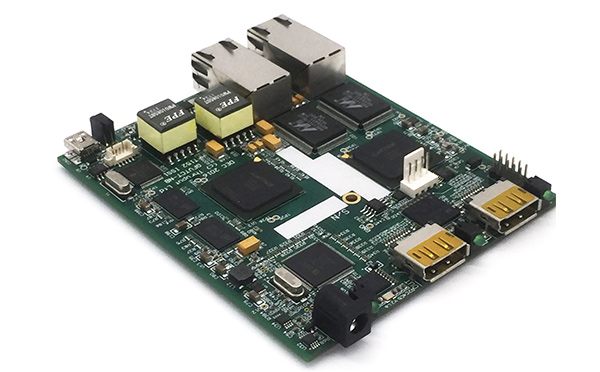
The daily double-sided PCB (printed circuit board) extended from the substrate surface to both sides are the line layer, welding resistance layer, character layer composition, and through the drilling layer through the top bottom line to achieve connected gas.
Use of solder resistance
(1) Prevent the damage of moisture and various chemicals and electrolytes leading to oxidative corrosion of the line and harm the electrical performance;
(2) Prevent external mechanical scratching, avoid contact short circuit and maintain good insulation performance of the board;
(3) To prevent the circuit board welding components, should not be welded part is connected to the solder and short circuit;
(4) reduce the loss of tin spray and gold deposition in non-welding areas;
(5) Cover the circuit board with various colors of ink to beautify the appearance.
Design of solder resistance
Choke welding, literally, means "stop welding," and some beginning engineers may think that the pattern on the choke welding is not soldable. This understanding is wrong. Welding resistance refers to the part of the board to be printed with welding resistance ink (mostly green ink, so welding resistance is also known as green oil), because it is a negative output, so in fact, the pattern on the welding resistance layer is not printed with ink, in order to make a metaphor for understanding:
A gazebo is like a solder shield. After a heavy snow, the ground blocked by the gazebo will not have snow (solder shield ink), and the ground not blocked by the gazebo will be covered by snow (solder shield ink). Following this idea, let's go back to PCB welding design:
1. Where there is a pattern on the line layer, the copper surface is made
2. The pattern of the solder resistance layer is not covered with ink
3. The place where the line layer overlaps with the solder resistance layer on the same side will make the copper exposure (spray tin or sink gold) effect
Fabrication of solder resistance
In actual production, after drilling and sinking copper on the board, the unnecessary copper surface is removed, and the required copper surface (that is, the line process) is retained. Then the welding resistance production process begins:
1. After etching the line copper surface grinding plate pickling treatment, remove the surface oxides and impurities, coarse copper surface to increase the bonding force with solder resistance ink
2. The whole board is printed on the solder resistance ink after drying, the solder resistance film is covered on the board, and the ultraviolet irradiation is used. The ink that is not blocked by the solder resistance pattern is cured on the board and can not be cleaned off
3. The next is development cleaning, welding pattern blocked ink cleaning, exposing the original copper surface, and then spray tin or gold in the following process
In the process of welding resistance, because of the alignment deviation of the machine, it is necessary to "welding resistance window welding pad greater than the line welding pad" (generally the overall size is about 0.1-0.2MM, that is, unilateral external expansion 0.05-0.1MM). In the actual production, there will be welding resistance window to make some welding plates deformed or too large, mainly reflected in:
1. When there is an independent line pad under the choke window, the actual shape of the pad: the shape of the line pad.
2. The actual shape of the welding pad when the line pad is connected to the line under the welding resistance window: the line pad + a small part of the connected line shows the shape of copper (part of the line shows copper in the welding resistance window).

3. The actual shape of the welding pad when the line welding pad is on the large copper surface is below the welding resistance window: the shape of the welding resistance window pad (the welding resistance window exposes part of the copper surface around the line welding pad to copper, thus making the pad larger)
The difference between welding aid layer and welding resistance layer
1.Paste assistant layer: Used in steel mesh factory to make steel mesh, so that the solder paste can be accurately printed on the patch pad to be welded through the steel mesh, and then SMT processing can be carried out
2.Solder solder layer: for PCB processing, do not print ink on the solder solder layer where there is a pattern, and print ink on the place without a pattern
Emphasize:
If you need a wire, copper surface or solder plate, do not need to cover ink and spray tin (or gold), you must add solder layer here, solder layer coincide with the copper spray tin (or gold).
Paste is just a layer of steel mesh, which is used to make steel mesh. It has nothing to do with the production of PCB, and PCB board factory engineering does not process or provide this file.
Fabrication of solder resistance bridge
For dense IC pads, in order to reduce the risk of short circuit caused by tin flow to the other IC pin during welding, a solder resistance bridge can be designed (that is, a layer of solder resistance ink is printed between two IC pads)


Just upload Gerber files, BOM files and design files, and the KINGFORD team will provide a complete quotation within 24h.