
Professional PCB manufacturing and assembly
Building 6, Zone 3, Yuekang Road,Bao'an District, Shenzhen, China
+86-13410863085Mon.-Sat.08:00-20:00

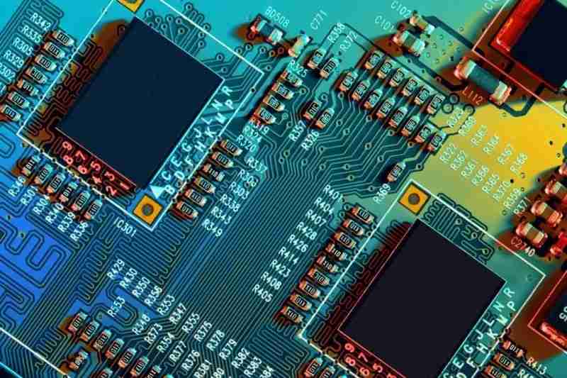
In PCB design, we often wonder whether the surface of PCB should be covered with copper? This actually depends on the situation, first we need to understand the advantages and disadvantages of copper surface.
The advantages of copper coating
1. Copper coating on the surface can provide extra shielding protection and noise suppression for the inner signal;
2, can improve a heat dissipation capacity of PCB board;
3. In PCB production process, save the amount of caustic agent;
4. Avoid PCB warping deformation caused by PCB overreflow welding stress caused by copper foil imbalance
The corresponding surface coating of copper also has corresponding disadvantages:
(1) The outer coppered plane will be fragmented by the surface components and signal wires. If there is poorly grounded copper foil (especially the thin long broken copper), it will become an antenna, resulting in EMI problems;
For this kind of copper skin, we can also dig through the function of the software
(2) If the pin of the component is fully connected with copper, it will cause heat loss too fast, resulting in diswelding and repair welding difficulties. Therefore, we usually adopt the copper laying method of cross connection for the patch components
Therefore, there are the following conclusions for the analysis of whether the surface is coated with copper:
1, PCB design for the two layers of board, copper is very necessary, generally to the bottom of the ground plane, the top put the main devices and walk the power line and signal line.
2, for high impedance circuit, analog circuit (analog to digital conversion circuit, switching mode power supply conversion circuit), copper is a good practice.
3. For multi-layer high-speed digital circuits with complete power supply and ground plane, note that this refers to high-speed digital circuits. Copper coating on the outer layer will not bring great benefits.
4. For multilayer digital circuits, there is a complete power supply and ground plane in the inner layer. Coating copper on the surface can not significantly reduce cross talk, but too close to the copper will change the impedance of the microstrip transmission line, discontinuous copper will also cause a negative impact on the transmission line impedance discontinuity.

5. For the multilayer board, the distance between the microstrip line and the reference plane < At 10mil, the return path of the signal is directly selected from the reference plane located below the signal line, rather than the surrounding copper sheet, because of its lower impedance. For double-layer panels with 60mil spacing between the signal line and the reference plane, the complete copper cladding along the entire signal line path can significantly reduce noise.
6, for the multilayer board, if the surface device and the line is more, do not apply copper, to avoid too much broken copper. If the surface components and high-speed signals are few and the board is relatively empty, in order to meet the PCB processing requirements, you can choose to lay copper on the surface, but pay attention to the PCB design between copper and high-speed signal line at least 4W distance, so as to avoid changing the characteristic impedance of the signal line
25 simple high speed PCB design tips
Jan 31,2023


Just upload Gerber files, BOM files and design files, and the KINGFORD team will provide a complete quotation within 24h.