
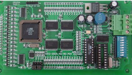
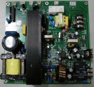
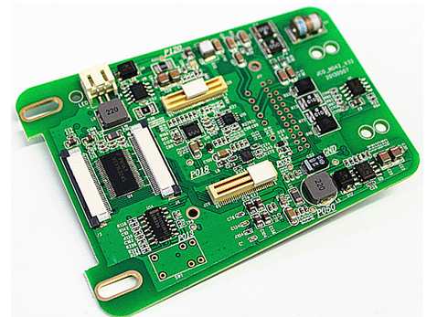
Professional PCB manufacturing and assembly
Building 6, Zone 3, Yuekang Road,Bao'an District, Shenzhen, China
+86-13410863085Mon.-Sat.08:00-20:00

PCB solder mask is the soldermask, which refers to the part of the board to be coated with green oil. In fact, the solder mask uses negative output, so after the shape of the solder mask is mapped to the board, it is not green oil solder mask, but copper skin is exposed. Generally, in order to increase the thickness of the copper sheet, the green oil is removed by scribing on the solder mask, and then tin is added to increase the thickness of the copper wire.
◆◆
Requirements for solder mask
◆◆
Solder resistance layer is very important in controlling welding defects in reflow soldering. PCB design should minimize the spacing or air gap around the pad.
Although many process engineers prefer to separate all pad features on the board with solder mask, the pin spacing and pad size of closely spaced components will require special consideration. Although the non zoned solder mask opening or window on the four side qfp may be acceptable, it may be more difficult to control the tin bridge between the element pins. For bga solder mask, many companies provide a solder mask that does not touch pads, but covers any features between pads to prevent tin bridges. Most surface mounted PCBs are covered with solder mask, but if the thickness of solder mask is greater than 0.04mm, the application of solder paste may be affected. Surface mount PCBs, especially those using closely spaced components, require a low sensitive solder mask.
Work production
Soldering resistance materials must be used by liquid wet process or dry film lamination. The dry film resistance welding material is supplied with a thickness of 0.07-0.1mm, which is suitable for some surface mount products, but this material is not recommended for close spacing applications. Few companies provide dry films that are thin enough to meet the close spacing standard, but several companies can provide liquid photosensitive solder resist materials. Generally, the opening of solder mask should be 0.15 mm larger than the pad. This allows a gap of 0.07mm on the edge of the pad. Low profile liquid photoresist materials are economical and are typically designated for surface mount applications to provide accurate feature dimensions and clearances.
◆◆
Introduction to welding flux
◆◆
The soldering aid layer is used for chip packaging and corresponds to the SMT chip component pad. In SMT processing, a steel plate is usually used to punch holes on the PCB corresponding to the bonding pad of PCB components, and then solder paste is applied to the steel plate. When the PCB is under the steel plate, solder paste leaks, which means that each bonding pad can be coated with solder. Therefore, the solder mask cannot be larger than the actual pad size, and it is better to be smaller than or equal to the actual pad size.
The required levels are almost the same as those of surface mount components, mainly including the following elements:
1. BeginLayer: ThermalRelief and AnTIPad are 0.5mm larger than the actual size of regular pads
2. EndLayer: ThermalRelief and AnTIPad are 0.5mm larger than the actual size of regular pads
3. DEFAULTINTERNAL: M-server
Effect of solder mask and flux
◆◆
The solder mask layer is mainly used to prevent PCB copper foil from being directly exposed to the air, playing a protective role.
The soldering layer is used to make the steel mesh for the steel mesh factory, and the steel mesh can accurately put the solder paste on the patch pad to be welded when tin is applied.
◆◆
Difference between PCB soldering aid layer and solder mask layer
◆◆
The two layers are used for tin coating and welding, not one for tin coating and one for green oil coating; Instead:
1. The welding resistance layer means that a window is opened on the whole piece of welding resistance green oil to allow welding;
2. By default, areas without solder mask should be painted with green oil;
3. PCB soldering layer is used for chip packaging.


Just upload Gerber files, BOM files and design files, and the KINGFORD team will provide a complete quotation within 24h.