
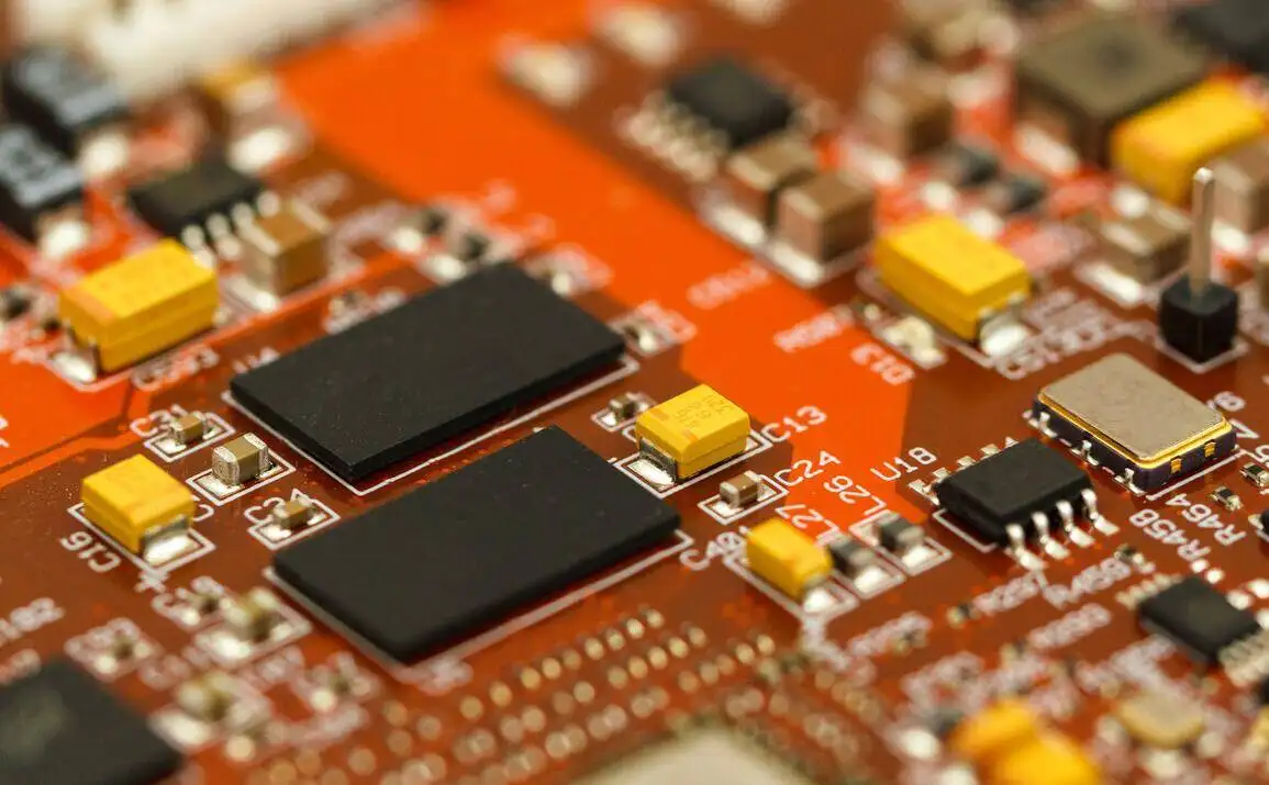
Professional PCB manufacturing and assembly
Building 6, Zone 3, Yuekang Road,Bao'an District, Shenzhen, China
+86-13410863085Mon.-Sat.08:00-20:00

PCB ground wire design plays an important role in circuit anti-interference design. Generally speaking, the main purpose of ground wire design is to determine the reference potential; The second is to eliminate the noise voltage generated when the branch current flows through the public ground wire, and avoid the influence of magnetic field and ground potential difference.
1、 Type of ground wire:
The grounding wires can be divided into several types, each of which has its own characteristics and functions, and must be distinguished in the design of grounding wires.
1. Digital ground is the reference point of zero potential of digital circuit. Because digital circuits generally work in pulse state, especially when the front and back edges of the pulse are steep or the frequency is high, it is easy to interfere with analog circuits.
2. Analog
It is the reference point of zero potential of analog circuit. Because the analog circuit not only undertakes the amplification of small signals, but also undertakes the power amplification of large signals, the analog circuit is easy to be interfered and generate interference.
3. Power ground is the reference point of zero potential of high current circuit. Due to the strong current and high voltage of this part of the circuit, the interference on the power ground wire is large.
4. DC power supply ground
It refers to the reference point of zero potential of DC power supply. Since DC power supply often supplies power to each unit in the system at the same time, and the power supply properties and parameters required by each unit may be very different, it is necessary to ensure that the power supply works stably and reliably, as well as that other units work stably and reliably.
5. Switching power supply ground refers to the reference point of switching power supply circuit. It is not isolated from the earth, and there is a potential difference between it and the earth.
6. Shielding ground is used to prevent electrostatic induction and magnetic induction. In most cases, it is connected to the ground together with the casing.
7. Safety grounding
Safety grounding refers to grounding the enclosure. The first is to prevent the accumulation of electric charge on the casing, which will produce electrostatic discharge and endanger the safety of equipment and personnel; Second, when the insulation of the equipment is damaged and the chassis is electrified, the power protection action is prompted to cut off the PCB power supply to ensure personnel safety.
2、 Ground wire design
Attention shall be paid to the following points in the design of ground wire:
1. Attention shall be paid to the relationship between the switching power supply ground and other ground: the switching power supply ground is the pulsating DC ground obtained from the mains through rectification. It is not isolated from the ground, and there must always be an alternating voltage. Therefore, for the common bridge rectifier switching power supply without power frequency transformer, its ground is always charged. At present, the sampling adjustment circuit of the switching power supply adopts a separate isolation sampling winding or optocoupler to isolate the ground of the switching power supply from other types of ground in the circuit, so that other types of ground are isolated from the mains power grid. Therefore, other types of ground can also be collectively referred to as cold ground.
2. Separate the ground of digital circuit from that of analog circuit. When there are both digital circuits and analog circuits on the circuit board, especially for high-speed circuits with a large number of digital circuits, they must be strictly separated. The usual method is to separate digital circuits from analog circuits. Generally, digital ground and analog ground are only allowed to provide one common ground in the circuit, and there cannot be multiple common ground points. Digitally, it is required that the wiring on the printed circuit board shall not be looped into a mesh to reduce the induced noise. When long distance parallel sections are unavoidable, shielding isolation shall be added between lines. To make the simulation scattering, take one point and connect it to this point digitally. The analog ground wire shall be thickened as much as possible, and the grounding area of the leading out end shall be increased as much as possible. In addition, high-level analog signals shall be isolated from low-level analog signals, both of which shall be separated from digital signals. Clock (digital signal) is as susceptible to noise as other analog signals, and it is also as susceptible to noise as digital signals, so it must be isolated from analog and digital systems.
3. Correctly select single point grounding and multi-point grounding. When the signal frequency is lower than 1MHz, because the electromagnetic induction between PCB wiring and PCB components has little influence, and the circulating current formed by the grounding circuit has a great influence on the interference, the single point grounding method can prevent it from forming a loop, so it is better to use single point grounding for low-frequency circuits. The single point grounding mode of multiple circuits is suitable for parallel connection. When the signal frequency is higher than 10MHz, the influence of the distribution parameters should be considered. Because the inductance effect of the wiring is obvious at this time, and the ground wire impedance becomes large, the circulating current formed by the grounding circuit is no longer the main problem. Therefore, multi-point grounding should be used to ground nearby, and the ground wire impedance should be reduced as much as possible.
4. Low power PCB design. The ground wire of high-power devices should be grounded separately, because there is a large current passing through the power ground, which is very easy to form a voltage drop on the printed circuit board conductor. If the wiring is not separated, the voltage drop will be introduced to the signal processing circuit to cause interference, and the high-power devices should be placed at the edge of the circuit board as far as possible to reduce the interference to the small signal processing circuit. In addition, some circuits (such as relays, transformers, etc.) generate high electromagnetic noise levels, and the interference to small signals is also very serious, so they should be grounded separately.
5. The grounding wire shall be thickened as much as possible. In addition to reducing the voltage drop on the ground wire, it is important to reduce the coupling noise. If the grounding wire is very thin, the grounding potential will change with the change of current, resulting in unstable signal level of electronic equipment and poor anti noise performance.
6. Ground plane in high-speed system. The ground plane not only provides a low resistance return circuit for high-frequency current, but also reduces the influence of external electromagnetic interference on the circuit. For example, the double-sided board, ideally, should have one side as the ground plane and the other side as the connecting layer, but in fact this is impossible, because usually there must be signal lines, power lines, etc. on the ground plane. Even so, reserve as much ground plane area as possible (at least 75%). In high-speed circuits, the grounding pin of all integrated circuits must be directly welded to the ground plane to reduce the inductance. Its power supply pin should be decoupled by a low inductance ceramic capacitor to reduce the impact on the formation. The ground plane must have no isolated ground, because if the grounding pin of the component is connected to the isolated ground, there will be no current circuit with the ground plane.
7. Grounding design of shielded cable. For the shielding layer of shielded PCB cable used for low-frequency analog circuit, it is better to adopt one point grounding method when grounding, and the grounding point of the shielding layer should be consistent with the grounding point of the circuit. The shielding layer of high frequency and digital circuit cables shall be grounded by multi-point grounding. When the cable length is greater than 0.15 times of the working signal wavelength, the interval multi-point grounding type of 0.15 times of the working signal wavelength shall be used. If it cannot be achieved, at least both ends of the shielding layer shall be grounded. If multi-layer shielded cable is used, each shield layer shall be grounded at one point, and each shield layer shall be insulated from each other. Circuits that are very sensitive to noise and interference or PCB circuits with particularly serious high-frequency noise should be shielded with metal covers. When using tubular capacitors, the enclosure should be grounded.


Just upload Gerber files, BOM files and design files, and the KINGFORD team will provide a complete quotation within 24h.