
Professional PCB manufacturing and assembly
Building 6, Zone 3, Yuekang Road,Bao'an District, Shenzhen, China
+86-13410863085Mon.-Sat.08:00-20:00

Sharing of pcb design step guide for electronic product design
The development of electronic product design can be divided into seven steps: preliminary production design, schematic diagram, PCB layout, final BOM, prototype, test and program, and final certification.
Step 1 – Create a preliminary production design
When developing new electronic hardware products, you should first conduct preliminary production design. Do not confuse it with a proof of concept (POC) prototype.
POC prototypes are usually built using development suites. Sometimes, they are useful in proving that your product concept can solve the problem you need. But the POC prototype is far from production design.
A preliminary production design focuses on component production, cost, profit margin, performance, function, development feasibility and manufacturability of the product.
You can use the preliminary production design to estimate the cost of each item of the product. It is important to know exactly the cost of development, prototyping, programming, certification, expansion, and manufacturing.
The preliminary production design will answer the following questions. Is my product feasible to develop? Can I afford to develop this product? How long does it take to develop the product? Can I mass produce products? Can I make money?
Many entrepreneurs mistakenly skip the preliminary production design steps and directly jump into the design schematic diagram.
In this way, you may eventually find that you have spent all these efforts and hard won money to buy products that cannot be affordable to develop, manufacture or, most importantly, sell profitably.
Step 1A – System Block Diagram
When creating the preliminary production design, the system level block diagram should be defined first. This figure specifies how each electronic function and all functional components are interconnected.
Most products require microcontrollers or microprocessors with various components (displays, sensors, memory, etc.), which are connected to the microcontrollers through various serial ports.
By creating a system block diagram, you can easily identify the type and number of serial ports you need. This is an essential first step in selecting the right microcontroller for the product.
Step 1B – Select Production Components
Next, you must select the various production components: microchips, sensors, displays, and connectors, based on the desired functionality and the target retail price of the product. You can then create a preliminary bill of materials (BOM).
You can purchase most electronic components (for prototyping and initial testing), or you can purchase up to thousands (for small volume manufacturing).
Once you reach a higher output, you will be able to save money by purchasing some components directly from the manufacturer.
Step 1C – Estimate Production Costs
Now you should estimate the cost of production (or cost of sales – COGS) of the product. It is important to understand the cost of making your product as soon as possible.
You need to know the unit cost of product manufacturing to determine the best sales price, inventory cost, and most importantly, your profit.
The production components you choose will certainly have a significant impact on manufacturing costs.
But to get an accurate manufacturing cost estimate, you must also include PCB assembly, final product assembly, product testing, retail packaging, scrap rate, returns, logistics, tariffs and warehousing costs.
Step 2 – Design Schematic
Now it is time to design the circuit schematic according to the system block diagram you created in step 1.
The diagram shows how each component from the microchip to the resistor is connected together. Although the system block diagram mainly focuses on higher level product functions, the schematic diagram only involves some small details.
Simple problems such as incorrect pin numbering on components in the schematic diagram can lead to a complete lack of functionality.
In most cases, each module of the system block diagram needs a separate sub circuit. These different sub circuits will then be connected together to form a complete schematic.
Use special electronic design software to create schematics and help ensure that they are error free.
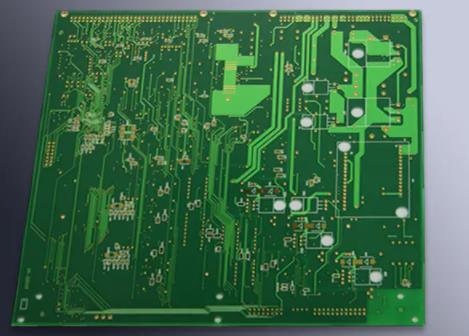
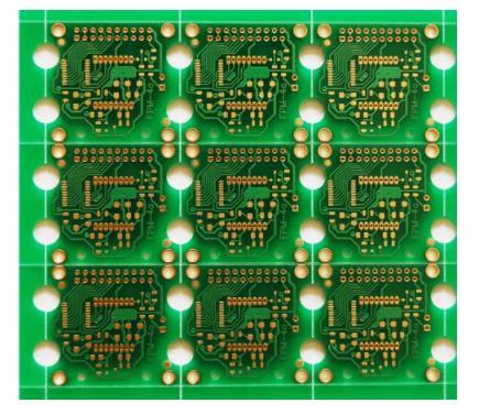
Step 3 – Design a Printed Circuit Board (PCB)
After completing the schematic, you will now design a printed circuit board (PCB). A PCB is a physical board that holds and connects all electronic components.
In essence, the development of system block diagram and schematic circuit is mainly conceptual. PCB design is a very real world.
Use the same software used to create the schematic to design the PCB. The software will have various verification tools to ensure that the PCB layout conforms to the design rules of the PCB process used, and that the PCB matches the schematic.
Generally, the smaller the product, the tighter the package of components, and the longer it takes to create a PCB layout. If your product routes a lot of power or provides wireless connectivity, PCB layout is particularly critical and time-consuming.
For most PCB designs, the most critical parts are power wiring, high-speed signals (crystal clock, address/data line, etc.), and any wireless circuit.


Just upload Gerber files, BOM files and design files, and the KINGFORD team will provide a complete quotation within 24h.