
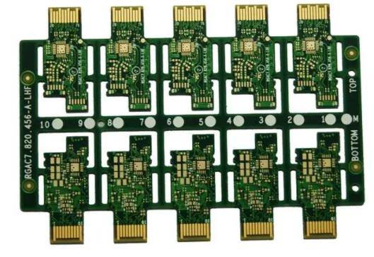
Professional PCB manufacturing and assembly
Building 6, Zone 3, Yuekang Road,Bao'an District, Shenzhen, China
+86-13410863085Mon.-Sat.08:00-20:00

Explain the single point grounding and multi-point grounding in PCB layout
Providing a good grounding system for PCB is probably one of the most important aspects of PCB layout. There are digital, analog, chassis and grounding. Their functions are important for the overall performance of the circuit board. The grounding system in the circuit board will perform all work, from maintaining a stable reference level to providing a clear return path for signals and currents.
We will study the single point grounding and multi-point grounding in PCB design, and the knowledge we need to know when connecting grounding in the next layout.
Single point grounding and multi-point grounding - which one?
Many different grounds can be used on the printed circuit board, one of the most common examples is the digital ground and analog ground on the mixed signal board. Grounding will need to be connected, depending on whether your design requires single point grounding or multi-point grounding. Let's explore both types.
Single point grounding
Circuit boards that are grounded differently from each other are referred to as single point or "star" grounding. This method is usually used in low-frequency applications, and there is a grounding point on the board, which is tied together. If it is a split ground plane, the digital and analog ground planes will be tied together at some point between the splits.
Multipoint grounding
This grounding strategy is used for boards that operate at higher frequencies. Not every grounding circuit is connected to each other at one point on one plane, but all grounding circuits are shared on the same plane. Different circuits are connected to a reference ground plane through a low impedance connection. Shorter connections help reduce EMI that may occur at higher frequencies.
Single point grounding system works better at lower frequencies, while multi-point grounding system works better at higher frequencies. In many cases, there is a mixture of single point grounding and multi-point grounding in the power supply network of the circuit board. However, some important points about how to connect the grounding system must be kept in mind to avoid problems, which will be introduced in the following content.
Incorrect configuration of grounding plane
If all the return current flows through a single point, a single point grounded system may cause problems. This interferes with the normal flow of high-frequency currents throughout the ground plane, thereby radiating EMI. In many cases, it is better for different circuits to share the ground plane and provide different return paths on another layer of the board. It is also important to keep signals close to their return path to reduce the magnetic loops they will cause.
Another problem with the separation plane is that it may cause a loop of ground current. By embedding traces or splitting planes, you may block the return path and inadvertently create a loop. It is best to maintain the integrity of the ground plane and avoid situations that would block the return path, such as high-density areas of vias, slots, or other planar obstacles. If there are separate digital and analog ground planes, it is generally recommended that they be placed on different layers of the circuit board without overlapping to help minimize the capacitive coupling between them.
In PCB design, you usually want to view all unrouted networks on the circuit board, and place routing and routing at the highest priority in your workflow. However, in practice, each signal has a return path that must return to the source through the reference plane. If the ground plane is not properly designed to conduct these return paths, the performance of the signal will be compromised. Therefore, the layout engineer must consider both the designed wiring and grounding.
An incorrectly routed wire may cause problems with the signal, while a poorly designed grounding strategy may risk the operation of the entire circuit board.
PCB Layout Best Practices for Ground Plane
Before starting the layout, you must set up the board with all the correct parameters and settings. Part of this process is to set the layer stacking configuration of the circuit board by balancing the manufacturing cost with the wiring density and signal integrity requirements of the circuit board. Sensitive signals will require stripline layer configuration, which may require wiring multiple power supplies, and as we have discussed, circuit board grounding is also a factor.
When laying out a board, you will need to determine the strategy for creating the ground plane. Typically, the ground plane is created by a process called pouring copper. The designer will draw the plane profile, and then the system will form the plane according to the parameters set for it.
After implementing the plane strategy, the designer can continue to route. Please keep the following basic rules in mind when routing coupled with reference ground plane:
Don't cross the split plane; You will block the clear return path of the signal and may generate a lot of noise on the circuit.
When routing sensitive signals, keep them on a layer as close as possible to their reference plane for coupling.
If you must change the layer, try limiting the layer to either side of the reference plane to maintain a clear signal return path.
If you have to go through more layers, use a grounded transition via next to the signal via to continue the signal return path.
For power and ground connections, use short and wide routing wires to reduce their impedance.
In order to design a circuit board with a good single point or multi-point grounding system, designers need to follow many rules. Fortunately, the PCB design tool you use has many functions built in to help.
Set up design tools for generating ground planes
As mentioned earlier, the Dynamic Shape Instance Parameters menu allows you to easily control how the ground plane is created or changed. However, there are other aspects of the power supply and grounding grid that also need to be controlled. These include the routing width and spacing used during cabling, and what type of through-hole will be used.
As you can see in the above figure, the grounding grid and power grid are grouped into a network category, where you can easily control their different parameters. The Constraint Manager uses a spreadsheet style interface that gives you complete control over the board's network, components, and many other aspects, from electrical properties to manufacturing rules. The Constraint Manager can import or export its rules, making it easy to quickly set constraints for a new design using existing rules in the new design. The PCB processing factory explains the single point grounding and multi-point grounding in PCB layout, and the knowledge needed to know when connecting grounding in the next layout.


Just upload Gerber files, BOM files and design files, and the KINGFORD team will provide a complete quotation within 24h.