
Professional PCB manufacturing and assembly
Building 6, Zone 3, Yuekang Road,Bao'an District, Shenzhen, China
+86-13410863085Mon.-Sat.08:00-20:00

Share and explain 4 expensive PCB design errors
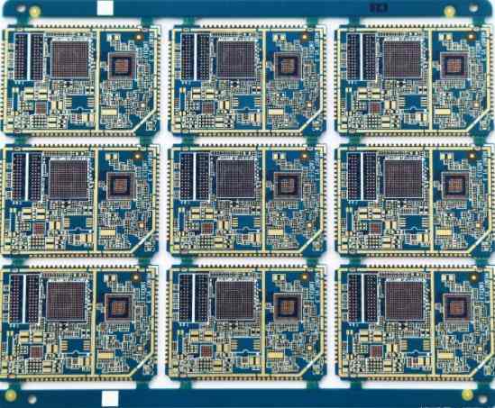
The design of printed circuit board is based on the circuit schematic diagram to realize the functions required by the circuit designer. The design of printed circuit board mainly refers to layout design, which needs to consider the layout of external connections. The optimal layout of internal electronic components, the optimal layout of metal wiring and through-hole, electromagnetic protection, heat dissipation and other factors. Excellent layout design can save production costs and achieve good circuit performance and heat dissipation. Simple layout design can be realized by hand, while complex layout design needs to be realized by computer aided design (CAD)
Printed circuit board design may be extremely complex, and mistakes made at this stage of the electronic design process may cause high costs. Our company is your PCB manufacturing partner and can help you in every step of the PCB manufacturing process (including the design phase). We provide free PCB design tools, such as FreeDFM, to check whether there are manufacturability problems in PCB design files before placing an order.
Although there are countless things that may go wrong in PCB design, we list four costly mistakes that need attention. More information about how our FreeDFM software can help you identify manufacturability issues in your design.
Check your PCB design for landing pattern errors
The landing pattern of the printed circuit board includes an electronic mechanism library using schematic symbols. If the design is thoroughly implemented, there will be no problem. However, if these libraries are not followed correctly, schematic symbols must be drawn manually. It is easy to make mistakes when manually drawing landing patterns, and this situation should be avoided as far as possible.
Avoid using too narrow high current wiring to create circuit board designs
The large current wiring must be wide enough to ensure normal flow. If forced wiring is necessary, it must be able to handle currents above several hundred milliamperes; In this case, the minimum width usually does not meet the requirements. Before production, measure the appropriate width for each PCB design.
The wire width calculator can help prevent errors in the correct width of the printed circuit board.
High speed routing in PCB design is too long
High speed signals can only follow the fastest, horizontal path available. Too long high-speed routing may cause the PCB to fail to work properly.
Check your PCB design for the best wireless antenna layout
The layout of the antenna is critical for correct wireless functionality. It can be said that this part of the PCB design process bears the greatest risk of error. The antenna and transceiver must be equal to achieve maximum power transmission. PCB processing factory explanation: PCB design may be extremely complex, and mistakes made at this stage of the electronic design process may cause high costs.


Just upload Gerber files, BOM files and design files, and the KINGFORD team will provide a complete quotation within 24h.