
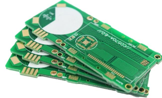
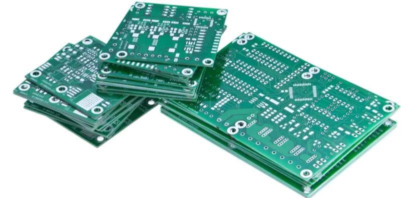
Professional PCB manufacturing and assembly
Building 6, Zone 3, Yuekang Road,Bao'an District, Shenzhen, China
+86-13410863085Mon.-Sat.08:00-20:00

Pcb design All information about PCB tool holes: their purpose and location
So many designers like to focus on PCB, but if you want to turn the design into a real product, you must consider the mechanical and manufacturing aspects of the design. PCB tool hole is an important mechanical function that can help you obtain design through manufacturing. The machined hole is different from the mounting hole, which is necessary to fix the plate to the workbench during the manufacturing process.
Although the tool hole may be the simplest function on a PCB, some basic guidelines should be followed when determining where to place the tool hole. After consulting the manufacturer about their panel and tool requirements, or if you decide to make your own panel, you can use the standard pad and hole functions in PCB design software to place tool holes. This is how it works and some of the best practices for using tools for machining in design.
Using PCB Tool Holes
Tool holes may be one of the simplest functions in a PCB, but they are critical to manufacturing and assembly. When determining the position and mode of the tool hole on the PCB, three key points should be considered:
Placement during panelization
Dimensions and Plating
Place with datum
Circuit board or panel?
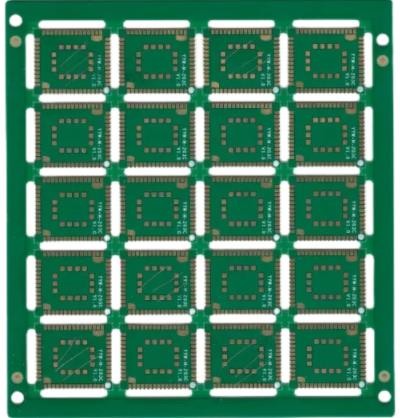
The first item that seems obvious is: Where should tool holes be placed? The tool holes are placed in the panel rather than on the circuit board, especially when the circuit board is placed in an array. It should be noted that the manufacturer is actually producing panels, not individual panels. PCB tool holes are used to aid manufacturing, so they should be placed in the panel. The following figure shows how to place the tool hole on the separation guide of the PCB panel.
If you want to design your own panel and separate rails, you can place PCB tool holes in the rail area or in the corner of the panel. The manufacturer I work with will accept customer panels that are suitable for their size, but they do not need you to submit the panels with the design documents. Typically, they will create their own panels, including PCB tool holes, and include them in their NRE costs. If you are sure you want to create your own panel, be sure to include the tool holes. Even if they are initially placed in the wrong position, your manufacturer can still fix the panels so that your circuit board can be manufactured.
I would like to point out that I have seen some suggestions, including placing tool holes directly on the finished PCB at the manufacturer. I am not sure if they intend to write "mounting holes" because they clearly refer to a single PCB, not a panel. Most guidelines, including those for pcb manufacturers and assembly plants, clearly indicate that tool holes should be placed on PCB panels. With this in mind, let's look at the differences between PCB tool holes and mounting holes.
Tool hole and mounting hole
Some guidelines will point out that tool holes and mounting holes are the same thing, but this is not necessarily correct. The main difference is electroplating: PCB tool holes are non electroplating through holes, while mounting holes are usually electroplating. Another difference is size: PCB tool holes usually have some standard imperial or metric sizes. Your manufacturer may recommend using specific PCB tool hole sizes so that your circuit board can be put into production without modification. The dimensions of the mounting holes are standardized only according to the mounting hardware used to mount the board to the chassis.
When the mounting hole is used with metal hardware, it should be grounded by connecting to the grounding wire or grounding plane/copper powder. The plated through-hole shall also have bare pads to provide low resistance electrical connections to the metal mounting base. The basic function of placing some additional grounding conductor on the board is to provide some additional shielding and prevent any floating conductor from generating stray capacitance. I prefer grounding to a larger copper pouring area or plane, because a larger metal mounting base can also act as a heat sink and pull excess heat out of the circuit board and into the shell.
Datum point
Another important point is the benchmark, which is used to ensure that the template printer, pick and place machine and automatic optical inspection (AOI) machine can determine the PCB direction. The datum shall be placed at 3 corners of PCB layout to make the direction of bare PCB clear. However, they should also be placed on the panel so that corners can be identified. For simplicity, simply place the reference point in the corner away from the PCB tool hole and follow the size recommendations of the assembler.
Place PCB tool holes
Placing tool holes is simple: simply use the "Place Pad" or "Place Hole" function in the design software. Excellent PCB CAD tools allow you to define specific holes as plated or non plated holes; Simply set the hole to non plated and set the desired diameter to complete the tool hole design. The PCB processing factory explains all the information about PCB tool holes in pcb design: their purpose and location, and some basic rules should be followed when placing the tool holes.


Just upload Gerber files, BOM files and design files, and the KINGFORD team will provide a complete quotation within 24h.