
Professional PCB manufacturing and assembly
Building 6, Zone 3, Yuekang Road,Bao'an District, Shenzhen, China
+86-13410863085Mon.-Sat.08:00-20:00

PCB Creepage and Clearance Criteria in Designing PCB Layout
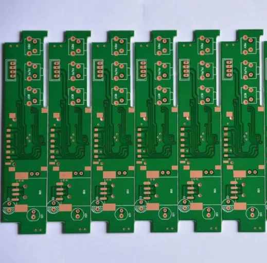
High voltage parts on printed circuit board
There are many bonfires, such as bonfires or fireplaces, which can improve productivity, warm and even romantic. However, you will never see a fire on the PCB. If the PCB design is not suitable for high voltage, this may be a real risk. In some cases, an improperly designed circuit board may generate electrostatic discharge, which may damage the circuit board and components, and may cause a fire.
To avoid this problem, PCB designers engaged in high-voltage applications should pay special attention to the separation between bare metal conductors in the design. There are two ways to measure this distance, namely creepage distance and clearance, and it is important to maintain the required distance between them. Here we will learn about the differences between PCB creepage distance and clearance standards, as well as the steps that need to be taken to avoid high voltage problems or PCB accidental combustion. The circuit board assembly and circuit board processing manufacturers explain the design methods that meet the PCB creepage distance and electrical clearance standards
Differences between creepage distance and electrical clearance of PCB
If the distance between metals is too close, printed circuit boards conducting high voltage may suffer from electrostatic discharge between exposed metals. This discharge may damage the circuit board and its components. For PCB designers, it is important to observe the proper spacing between metal conductors on the circuit board. The conductor spacing on the circuit board can be measured by two methods: creepage distance and electrical clearance:
Creepage distance: It refers to the distance between two conductors on the surface of circuit board or insulating material.
Gap: This is the line of sight distance between two conductors through the air.
In high-voltage circuit with voltage higher than 30VAC or 60VDC, the rules of creepage distance and electrical clearance interval must be observed to prevent accidental arc between two conductors. Generally, these two measurements are the same, just like the distance between two component pads or other exposed areas of metal on the accessible part of the board. However, in some cases, the two measurement methods will be different, depending on the placement of the components or whether the contour of the bare plate is abnormal. As shown below, the creepage distance refers to the distance between the circuit board surfaces between two component pads. On the other hand, the gap is the air gap between the metal radiator of the left component and the cushion of the right component.
As shown in the side view, examples of creepage distance and electrical clearance on PCB
Next, we will study where we can find these creepage distance and clearance standards.
What are PCB creepage and clearance standards?
The calculation of PCB creepage distance and clearance criteria requires consideration of different factors, including operating voltage, pollution level (dust and condensate on the circuit board), and the type of circuit to be evaluated. Another important factor in the calculation of creepage distance is that the layer material is used to construct the original plate. The voltage will form a conductive path on the surface of the circuit board, which will damage its insulation performance. Some circuit board materials are more resistant to this effect than other circuit boards. The comparison tracking index (CTI) defines the resistance value of each material; The higher the number, the greater the puncture resistance. For example, the default CTI value of FR-4 is 175, while the CTI value of other more professional materials can be as high as 600.
There are many documents related to PCB creepage and clearance standards, the main document is IPC-2221. This is a generic standard that covers many different design rules, including the spacing required for high voltage circuits. These limits are described by the DC or AC voltage level, the inner layer, the coated or uncoated outer layer, and the substrate material. In addition to IPC-2221, you can find additional information in these standards:
IPC-9592: This standard is more specific than IPC-2221 because it defines the spacing requirements for power conversion equipment higher than 100 volts.
UL-61010-1: These standards specify safety requirements in the design of electrical testing and laboratory equipment and other industrial equipment.
UL-60950-1: This standard is applicable to high and low voltage applications of various equipment.
These standards will provide a solid basis for setting the gap required for the PCB to protect the PCB from overvoltage events that may create an arc between two different conductors. It is also important to simulate the power distribution in the design and use these results to help set the physical properties of the layout.
Layout of power supply components on the circuit board
How to use these standards to design PCB layout
After the spacing requirements are met, the circuit board will need appropriate creepage distance and electrical clearance. The next step is to set these values in the design rules of the PCB layout system. Rules and constraints can be set for the gap between metals, whether between routing, pads, copper pouring, or any combination of the three. You will also need to set the correct spacing for the space your components take up, especially for larger components that carry a large amount of voltage. In some cases, you can even set a unique avoidance gap around a specific space to solve the problem of radiator and other abnormal configurations. All of these rules will help you maintain the necessary spacing between the required high-voltage components.
When you place components in the layout, make sure that when you take them into consideration all aspects of the part. This will include any metal conductors (such as radiators) that may overhang the part, especially if you cannot set a unique avoidance area around the part. During layout, you also need to ensure that any edits or changes to component placement do not exceed the spacing you have carefully set between parts. Even rotating the assembly 90 degrees will cause abnormally shaped parts to violate the voltage gap.
These are two other techniques to consider when placing spacing:
To help maintain the correct spacing, try placing high-voltage components on one side of the circuit board and low-voltage components on the other side. In some cases, the spacing rules between high-pressure parts may not be as strict as those for low-pressure parts.
Creepage will require another solution because placing parts on the other side of the board will not give you the isolation you need across the board surface. Instead, you may want to install insulating barriers or cut grooves or slots in the board. The change in the board profile will increase the distance across the entire surface that the voltage must travel, providing you with the required creepage distance.
Fortunately, your PCB design tool has many functions that can help. We will introduce them in the following content.
Rely on the powerful functions of PCB layout tools
Setting design rules and constraints is the best way to ensure that the layout complies with PCB creepage and clearance standards. The Constraint Manager in the PCB Editor can be set using a specific footprint to encapsulate gaps to maintain the correct creepage distance for high-voltage parts. In addition, you can create grid classes for power and ground grids and assign them the necessary spacing. These settings, when used with design rules, will help you maintain the desired spacing.
You should also make full use of the circuit simulator and analysis tools that come with the PCB design system. These can be used to model the distribution network of a circuit board to ensure that the high-voltage network is connected according to your needs. Finally, be sure to use the 3D view and check functions in your PCB design tool. Parts that conduct high voltage may have irregular contours, such as heat sinks, and the ability to inspect them in 3D and visually confirm their location is an important asset for your design.


Just upload Gerber files, BOM files and design files, and the KINGFORD team will provide a complete quotation within 24h.