
Professional PCB manufacturing and assembly
Building 6, Zone 3, Yuekang Road,Bao'an District, Shenzhen, China
+86-13410863085Mon.-Sat.08:00-20:00

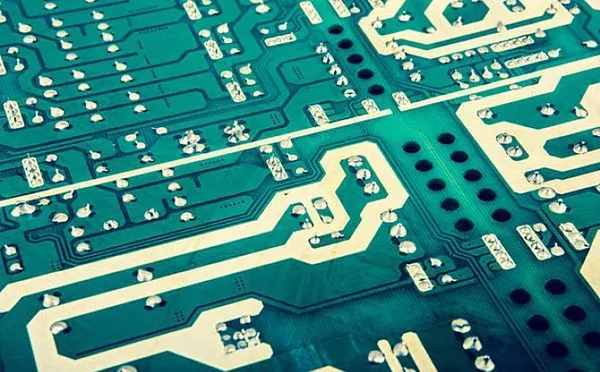
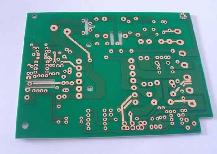
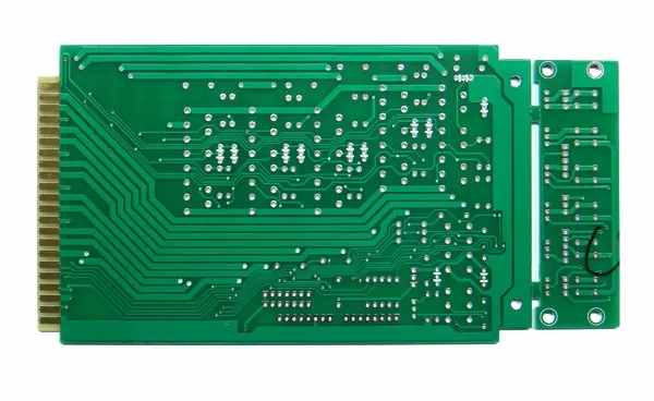
High current wiring in PCB layout via via sewing
The same general warning rules apply in circuit board design. High current is a necessary condition for design, but if you do not pay due attention to PCB layout, it may also lead to some unpleasant consequences.
Power and ground must be managed in the design and correctly assigned to the different components to which they are connected. One technology used to manage high current in PCB layout is to sew vias, which can help transfer heat and energy of current through the circuit board. This is more information about using via stitching to handle high current routing in the next PCB design.
High current problem on the circuit board
Many systems consume a lot of power in their operation, and the circuit boards in these systems will need to conduct large currents. However, if the circuit board is not designed correctly for this current level, it may fail electrically or structurally. For example, a circuit board does not use enough metal to conduct current through its power supply layer, and the wiring may become overheated. If the heat dissipation is not correct, it will affect the normal operation of components not specially designed for it. Finally, the heat will produce a domino scene, and more and more parts will be affected, eventually leading to circuit board failure.
Another example of a high current that may adversely affect a circuit board is a physical failure of the circuit board structure. The materials used in the original circuit board manufacturing can withstand a lot of heat, but only a certain degree of heat. FR-4 is a standard material for PCB manufacturing, and the glass transition temperature (Tg) rating is 130 ℃. Beyond this point, its solid form will become unstable and may start to melt. However, even before this temperature is reached, heat may eventually burn through any thin metal trace on the board, resulting in an open circuit, such as a blown fuse.
In order to avoid these and other high current problems, it is necessary to carefully design these circuits in PCB layout.
Short and direct power supply and analog routing between components
Electrical and thermal considerations for high current circuits
High current will generate a lot of noise on the circuit board, especially the current related to switching power supply. The switching between on and off states will produce EMI, and the strength of EMI will increase with the increase of the rise time of the switch. Although this problem can be solved, the following PCB layout techniques aimed at reducing noise can also be used to control this problem.
The components in the power supply circuit shall be placed close enough for short and direct wiring connection without breaking the following design for manufacturability (DFM) rules:
The power supply components shall all be located on the same side of the board to eliminate the need for wiring inside the board.
The high current components of the power supply (such as inductors and ICs) should be as close as possible to achieve the shortest connection.
Put the components together like this, and the wiring should be very direct in the power supply unit. You will want to route as wide as possible to maintain a low inductance and reduce the likelihood of EMI.
This strategy will enable you to better control the electrical and thermal problems of high current in the power circuit, but there is still the problem of routing the high current to other points on the circuit board. The thermal problems in such high current wiring will require more metal, which may require wiring on more than one layer. Here, it is helpful to use sewn vias in high current wiring.
Power wiring of wiring stitched to another layer with three through holes
High current wiring can be formed in PCB layout through via stitching
When routing high current wires, it is always best to use as much metal as possible to reduce heat and inductance. However, in many cases, there is not enough space on the board to make the power cord reach the required width. The solution is multi-layer wiring on the circuit board. By stitching the routing and vias on different layers together, you will effectively multiply the current carrying capacity by the current carrying capacity on the single layer. In the above figure, you can see the power supply wiring on the internal layer of the circuit board. There are three sewing vias, which can be connected with the matching wiring on the adjacent layer. This frees up space for other wiring or other components on the external layer of the board.
It should be noted that a large amount of heat will be generated in the high current wiring. By stitching multiple power cords and vias on the inner layer together, you will provide a way for more metals to share heat, but still need to conduct heat dissipation. This can be done through a thermal via, which transfers heat to the metal pad on the outer layer of the board for cooling. The more heat dissipation you can provide for high current wiring, the better the performance of the circuit board and the less likely it is to suffer from thermal damage.
When planning and designing, we should also keep in mind some other layout problems that need to be considered at present:
PCB manufacturing: If your circuit board is to operate very hot under high current, it is better to explore other materials that can withstand higher operating temperature. Although these materials may be more expensive, they may save you money in the long run by avoiding heat related problems. You should also work with manufacturers to develop the best layer stacking configuration and power plane strategy for high current boards.
Plate thickness: by increasing the plate thickness, the weight of copper can be increased, so that the wiring is thicker. This allows you to reduce the routing width, leaving more space for routing and component placement. As with any manufacturing issues, these changes should be agreed with the manufacturer before they are included in the design.
Automatic assembly: As we have seen, higher current requires more metal due to current and electrical reasons. However, at the same time, the same metal that will emit unwanted heat during operation may also cause problems for PCB assembly. Large area of metal will lead to thermal imbalance of smaller parts, thus affecting their welding. To avoid this, be sure to use heat sinks when connecting parts directly to wide wires or large areas of metal.
Component placement: If it can be avoided, components with high current and high temperature should be placed at the edge of the circuit board. By placing more of these parts in the center of the circuit board, more space can be provided for the natural heat dissipation of the circuit board.
Take full advantage of your PCB design tools when routing high current cables
Routing PCB usually requires multiple routing widths and vias, depending on the content to be routed. Signal wiring requires thinner wiring and smaller through-hole, while power and ground wiring is usually the opposite. Sometimes, different power grids will require different widths, depending on the level of current they carry. To help layout designers cope with these challenges, PCB design tools usually have a constraint management system to set line width and spacing rules.
With the Constraint Manager, you can set rules for high-speed design topologies and trace lengths. You can also create rules for PCB assembly to control the spacing between components or how solder resist should be applied to fine pitch components. There is even a section where you can set electrical rules so that you can design based on the timing and delay values of the signal. With the versatility of the Constraint Manager, you will have the power required for wiring by stitching vias to achieve high current routing in PCB design.


Just upload Gerber files, BOM files and design files, and the KINGFORD team will provide a complete quotation within 24h.