
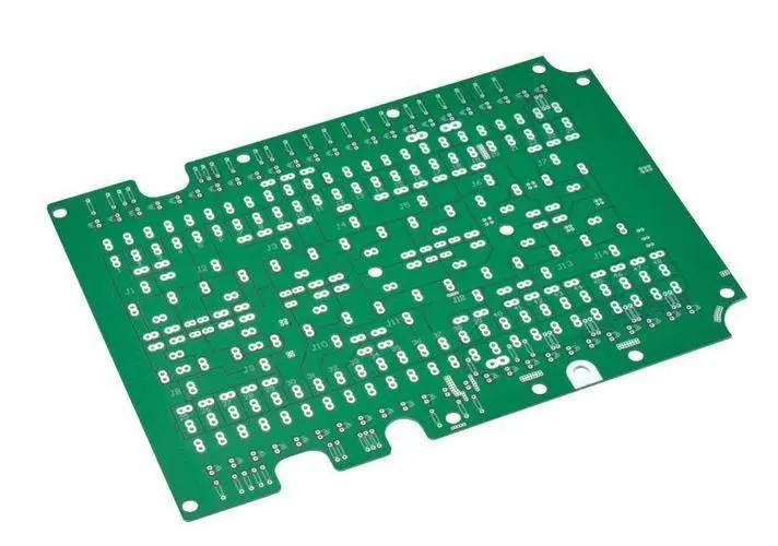
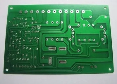
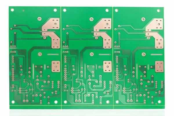
Professional PCB manufacturing and assembly
Building 6, Zone 3, Yuekang Road,Bao'an District, Shenzhen, China
+86-13410863085Mon.-Sat.08:00-20:00

What is printed electronic design? PCB company shares for you
What is printed electronic design? The answer is simple: it's electronic design. You use circuit theory, mathematical calculations, and computer-based simulations to design electronics. You use printed electronic materials to design electrical functions and performance for your products. Materials are key because materials used for printed electronic products have different electrical performance characteristics from materials used for traditional PCB. In addition, electronic products are manufactured in different ways using printed electronic materials. It is well known how PCB routing is completed. First, the electronic engineer designs it, defines the size according to the electrical requirements, and issues the manufacturing documents after the design is ready.
In the manufacturing process, the PCB is manufactured by copying the circuit on the copper of the PCB according to the design document, for example, by exposing the masked UV sensitive photoresist film to UV. Copper that was not exposed to ultraviolet light was then etched. The result is a trace of design. The dimensions are correct and meet the electrical requirements. In printed electronic products, we need to achieve the same results, but we need to adopt new design rules, materials and manufacturing methods.
The input and output of printed electronic design are basically the same as PCB design. The same technique applies between input and output: electronic design. You need to incorporate material information and design rules into your design process, and the output is a manufacturing file. The same physical laws are effective in the electronic design of PCB and printed electronic products, and they set the boundaries of what can be done. Two circuits, one made of PCB and the other made of printed electronic products, can have exactly the same function, but the circuit design looks different from the actual one. This is due to the physical capabilities and limitations of the materials used in the circuit. In both circuits, you need to apply a voltage difference across the impedance to allow the current to flow. To get the same current in both circuits, you need to adjust the impedance to the same level or set the voltage level specific to the circuit. These parameters are usually required to play a role in the printed electronic design. We are looking for the best solution by fine tuning the impedance and setting the correct voltage level.
In electronic design, it is very important to understand the material characteristics of the final product. From PCB, you can learn about copper thickness, thin layer resistance, its thermal properties, dielectric constant of PCB materials, etc. This is exactly the same parameter you need to know from printed electronic products. What is the final thickness of the silver ink conductor, what is its square resistance, and what is the dielectric constant of the substrate material? You perform electronic design for these new materials. Ohm's law, Kirchhoff's circuit theory law and Maxwell's equation are also applicable to printed electronic products. There are hundreds of different conductive inks on the market, each with a unique square resistivity. Some inks have high conductivity (usually still much higher than pure copper), but after curing, these inks cannot stretch at all. Other inks can stretch after curing, but the conductivity is worse. In electronic design, it is important to know what the square resistance of the ink used after final curing is.
Another design challenge is that the material parameters used in printed electronic products depend on the products used. For example, how to print conductive inks, how to cure these inks, and how other printing inks below the conductor affect the final square resistance. You may need to change your layout design for production. Otherwise, the production must be set according to the circuit requirements you designed. It is very important to understand the manufacturing methods of printed electronic products. There is no difference in PCB. You need to know how these are built and what the limitations of this specific production are. However, in PCB, the manufacturing methods are more standardized. Each manufacturing is basically similar, but the capabilities are slightly different. In the field of printing and electronics, we have not reached this level.
Conductive ink can be printed in many ways. The most common methods are screen printing and ink-jet printing. You can find many other methods through Google search. The key to the printing process is to understand manufacturing capabilities and their limitations. What is the minimum clearance required between runs? How many conductive layers can you use? What is the minimum and maximum width of the routing? Be familiar with the design rules of the product you will use, and check the design according to these design rules. Many of the design rules available in PCB design tools can be used in printed electronic design with correct rule definitions. If manufacturing includes design rules that are not supported by electronic design tools, it means that you must perform manual design rule checks. For example, if you can use multiple conductive layers separated by printed dielectrics, this means that your design rules between the first and second conductive layer routing are exactly the same as those printed on the same layer. And this is not a supported standard PCB design tool.
In addition, printed electronic products require components to obtain functions, and assembling components on printed electronic circuits is not a standard welding process. The typical material used in printed electronic products is plastic, which means that these thermal characteristics are different from those of PCB or FPC. This means that the adhesive material is also different. Low temperature solder, conductive adhesive or other adhesive materials are typical materials for printed electronic SMAs, which may require special packaging of components. Can you put the trace under the component? Do you need a special restricted area? What components can you install on a printed electronic device? Compared with SMA of PCB, these are problems that need to be considered from different perspectives. In addition, the manufacturing documents of surface mount components may be different. Can you paste the template file or should you provide a dispensing chart instead? Check SMA requirements in advance.
Because printed electronics is a fairly new technology field, information on material properties and manufacturing methods is not as available as PCB. In addition, there are a large number of conductive printing inks with different electrical characteristics, depending on the characteristics of the manufacturing equipment and method in the ready-made components. The design depends on the electronics theory of realizing new materials and manufacturing methods. For me, electronic design means using theory, physics and mathematics to ensure electrical function and performance. These methods require material knowledge as input. I see a lack of material information in printed electronic products, and sometimes decisions are made without calculation. Then it is not design, but speculation. Circuit board assembly and circuit board processing manufacturers explain how to use circuit theory, mathematical calculation and computer based simulation to carry out electronic design.


Just upload Gerber files, BOM files and design files, and the KINGFORD team will provide a complete quotation within 24h.